This post covers CMOS formation techniques. There are a few CMOS formation technologies:
1. P-well process
2. N-well process
3. Twin-well process
4. Triple-well process
P-well and n-well processes are similar. Technically, the p-well process appears before the n-well process.
Wells are required regions of doped silicon. Doping variations can be reached with processes like implantation, epitaxy or deposition.
The ion implantation process lies in the fact of bombarding the silicon layer with the beam of particles of high energies. The advantages of ion implantation are low temperature, precise control of the implantation dose, and resistance to the surface cleaning processes.
When the energised atoms reach the Si surface, they go inside the substrate, creating regions with different doping density. The temperature of the process is usually kept as low as possible to prevent diffusion of the impurities from the regions with high concentration to regions with low concentration. Low temperature helps to control the implantation process. Figure below briefly shows the implantation process.
Epitaxy is the process of growing a single crystal semiconductor layer on the top of another crystal (in this case this is silicon). It is usually used for growing multiple layers for integrated circuits, manufacturing and also for LEDs. Figure below shows schematically the process of epitaxy.
Deposition or chemical vaporation deposition (CVD) is the process where a semiconductor material deposits from the vapour phase onto the surface of the semiconductor wafer. The result of CVD is the thin film or single-crystal layer on the wafer surface. This process can also be used to produce latter layers of the CMOS process.
A detailed explanation of these three CMOS fabrication processes is provided in the Nanoelectronics module of this course.
Let’s consider the n-well CMOS process in the example of the nMOS transistor. The substrate is usually grounded to keep the p-n junction reverse-biased. The n-well can also be used as a resistor (under the condition where both resistor contacts will have a large enough voltage to keep the p-n junction reverse-biased). CMOS ICs are formed by patterning the semiconductor and other layers on and in the substrate.
Applying the process described above, we will use the following masks, that determine the space where device components will be on the chip:
1. n-well process
2. polysilicon process
3. n+ diffusion
4. p+diffusion
5. contacts
6. metal
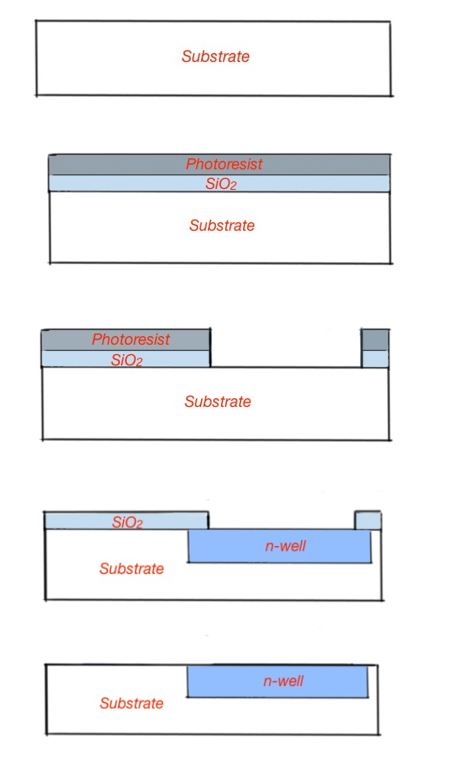
The CMOS fabrication process starts with the creation of a n-well in the p-type silicon substrate. This process is schematically shown in Figure 3. The first five electron donors should be added to the p-type substrate to create an n-well.
To define the regions of an n-well, the layer of oxide should be deposited on the wafer. The wafer oxides are in a high temperature (~1,000°C) to create .
After that the should be patterned with the layer of photoresist, that softens with light.
The photoresist and oxide layer is removed through the n-well mask, with a special mix of acids – sulfuric acid and hydrogen peroxide, that is called piranha etch. After removing the dioxide and etch, the n-well should be doped. There is two ways to do that – implantation and diffusion. In case of diffusion, the structure goes to the oven with the doping gas. The dopant atoms diffuse the substrate. Note that the well can be slightly wider than the etched space because of the effect of lateral diffusion. In the case of ion implantation, the dopant atoms, accelerated with the electric field, bump into the substrate. The oxide prevents the dopants go to the wafer, so the well fabricates only in the regions where it is needed. The oxide layer dissolves with the HF acid.
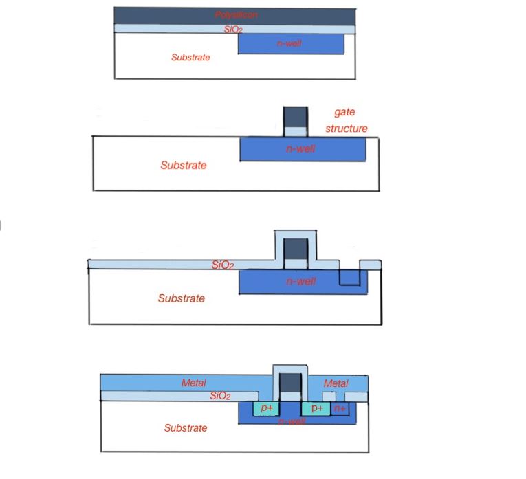
The formation of the transistor gate is depicted in Figure below. The transistor gate formation requires the polysilicon layer to be on the surface over the layer of oxide on the top of the wafer. It can be grown in the way as described above. After that the wafer with oxide layer goes to the reactor with silicon gas where the polysilicon grows with the method of chemical vapour deposition (CVD). After that the wafer becomes patterned with the polysilicon mask for gates formation, with the way described here.
The next step is n+ region formation, that will work as an active area of a transistor and the coll contact (Figure 4). First the oxide layer forms on the surface of the structure, then it patterns with the n-diffusion mask. So we expose only the area where the n+ regions should be. The N+ region formation goes with the ion implantation process. The oxide layer dissolves (Figure below).
The p-diffusion process goes similarly to the n-diffusion to create p-region in the wafer. Afterwards the structure should be covered with the field oxide and patterned with the contact mask, that is needed for contacts formation. The thick oxides cover all the wafer surface except the places where contacts should be. Then aluminium is applied on the whole surface of the wafer. The plasma etching process removes metal everywhere except the places where contact pads to the transistor should be (Figure below).
This is a very basic description of the transistor formation. Modern fabs use more complex techniques, with a bigger amount of layers on the structure using a more detailed technology with different parameters of the formation process. However, the mask principle remains the same.
The fabrication process should be made with the layout design rules. Usually the commercial manufacture is scaled with μm. Sometimes the simplified scalable design rules are used. The Mead and Convey rule in the VLSI design, are mostly used in universities due to its simplicity and uniformity. It is based on the scalable parameter
The parameter describes the process scale, which is equal to half the distance of the transistor channel. For example, if the process is 180nm, then the design rule is .
For example, the 180nm technology MOSFET was designed by the group of researches from Polytechnical University of Lausagne (Ecole Polytechnique Federale de Lausagne) using Verilog. The code presented by the research group is not for commercial and industrial use, but it may be used for simulations. The supporting documentation for the code is also presented on the university website.
Educational content can also be accessed via Reddit community r/ElectronicsEasy.
(III-V semiconductor materials and devices”, R.J. Malik; Molecular Beam Epitaxy: From Research to Mass Production”, Elsevier Science; “CMOS VLSI design”, 4th edition, Neil H.E. Weste; “CMOS: circuit, design, layout and simulation”, 3rd edition, R. Jacob Baker. https://ekv.epfl.ch).