
This post covers topic of photolithography process. Before we considered how the simplest CMOS devices work. Every electronic engineer should understand how the devices he designs are manufactured. Let’s consider the fabrication technique step-by-step.
All the steps of semiconductor device fabrication occurs at the so-called fab (the technological cluster equipped for semiconductors manufacturing). The fab is a significant investment from a cost point of view – right now there is around 13 technological clusters for full semiconductor fabrication processing.
The most famous and biggest among them are TSMC in Taiwan, Global Foundries in the US, UMC in China and Samsung in Korea. Many fabless manufacturers use these fabs for their production needs. TSMC maintains a leading role in the world, investing significantly in R&D.
The 5nm and 7nm CMOS Technologies are already in their pipeline, while R&D work is being made beyond 5nm technology. The company has also presented their road-map for the upcoming years.
TSMC focuses on the transistor and technologies like strain-engineered CMOS, 3D structures,, high mobility materials and 3D IC devices. The foundry also works with research and academia studies. The Major TSMC projects are in 7nm and 5nm logic platform technology and applications, 3D IC, next-generation lithography and other long-term research of NVM, MEMS, RF and analogue SoC devices.
TSMC introduced the first SoC process technology in 2011. This technology manufactures MEMS by integrating TSMC and wafer stacking technologies. TSMC presents sensor technology ranges from 0.5-0.11μm for applications like G-sensors, gyroscopes, MEMS-microphones, pressure gauges, microfluidic and others.
TSMC first presented Si-pillar wafer level chip scales packaging (WLCSP) technology in 2016. TSMC offer the most comprehensive CMOS image sensor process technology portfolio with the node from 0.5μm to 40nm node for applications like PC cameras and recorders, TV systems and portable devices. The TSMC foundry provides the most low noise, and high accuracy.
Another large and leading foundry is Global Foundries, the leading full-service semiconductor design, development, fabrication and innovation company in the US. As the Taiwan foundry above, it works with different companies interested in developing unique semiconductor products, and having 250 customers all over the world, including the largest semiconductor companies in the world. They have five 200mm fabs and five 300mm fabs in production. Global Foundries are moving forward the leading CMOS technologies of FDX, mainstream and embedded memory; RF technologies like SiG HP and PA, RF SOI and CMOS, ASICs technology and silicon photonics.
The United Microelectronic Corporation (UMC) foundry, based in Taiwan, is another global semiconductor foundry offering advanced IC products. The UMC’s foundry offers its customers solutions of 28nm gate-last High-K/Metal Gate technology, 14nm mass production, ultra-low power platform processes (that are in use in IoT applications), and also capabilities for automotive, with its highest rated AEC-Q100 Grade-0 of ICs. UMC has several advanced 300mm fabs, some of them manufacturing 14 and 28nm products, seven 200mm fabs and one 150mm fab.
The most famous fabs also belong to Samsung, SMIC, Powerchip, Vanguard, Huahong-Grace, Dongbu, TownJazz, IBM, MagnaChip, and WIN. Many of these companies are located in the Asia region. We will review in detail the processes and technologies that these fabs are offering, when we discuss the basics of CMOS fabrcation.
The first step is wafer fabrication. Wafer is a silicon (sometimes silicon carbide). A silicon wafer is cut from silicon boules. The wafer should be very thin (less then 1mm) in accordance to a process. Boules manufacturing is also a chemical process. They are a single-crystalline silicon, manufactured by pulling from molten silicon.
The size of the boules (or wafers later on) is up to 300mm. The method of silicon boules manufacturing is called as Czochralski method. The silicon electrical properties are obtained by impurities control. The seed goes into the molten silicon to start the crystal growth with the same orientation of the crystal as the seed. The temperature of the process is kept a few degrees higher than the temperature of melted silicon, to prevent it oxidising. After the seed is taken away during the rotation process, so the silicon recrystallises.
The next step is the preparation of the layer structure of a semiconductor device. The remaining semiconductor layers are prepared with the method of photolythography. In a few words, photolythography process is a mask method that enables the prevention of the ion implantation processes of the materials.
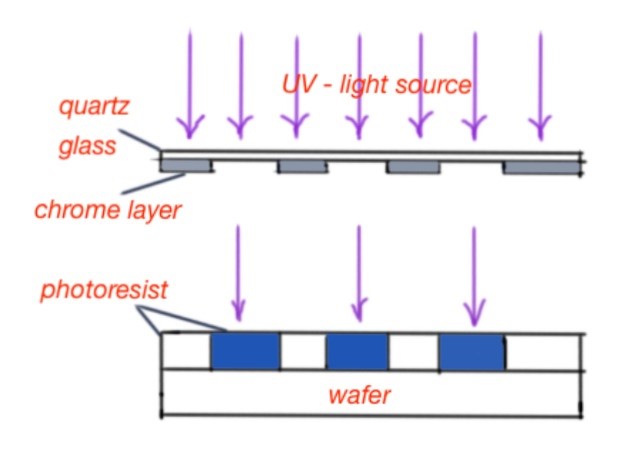
At first the wafer is covered or coated with photoresist, which can disappear under certain conditions. The next step is to use a photomask (Figure 1). The photomask is a quartz glass, with applied chromium material with a certain pattern. The photoresist is exposed by an applied UV source, where the mask is not covered by chrome.
An unexposed photoresist can be removed by the solvent, leaving the exposed photoresist layers on the wafer. There is also a photoresist that is initially dissolvable. The locations of this photoresist are applied with the UV light and are soluble. This type of photoresist is called positive photoresist, the first one – negative photoresist. The photomask is called a reticle. The stepper moves the reticle across the wafer. The most recent method that is used in photolythography process is projector printing.
The pitch of the printed mask is , where is the UV light source wavelength, is the refractive index of the medium, and is the acceptance angle of the lense. The parameter is the numerical aperture. This parameter is different for different manufacturing processes. Another important parameter is the depth of focus .
The term of the critical layer becomes very important with recent techniques. Wavelengths that are comparable or bigger than the feature size cause distortion in the exposed photoresist.
https://www.globalfoundries.com
http://www.umc.com
IC Insights, “Top 13 foundries Account 91% of Total Foundry Sales in 2013”, The 2014 McClean Report.
“CMOS VLSI design”, 4th edition, Neil H.E. Veste, David Money Harris.