This post covers the topic of CMOS logic. Si is a semiconductor, the basis for building most semiconductor devices. It is a IV group element, characterised by the covalent bond and three-dimentional cubic lattice. All these valence electrons are involved in the chemical bonds, and basically Si is a bad conductor.
Si conductivity can be changed by adding some inpurities into the structure, called doping. If the dopant is an element of V group, like Arsenic, then we get an n-type semiconductor, as there are free electrons in the structure. Doping by the III-group dopant such as boron, creates p-type semiconductor with holes, positively charged, in the semiconductor structure.
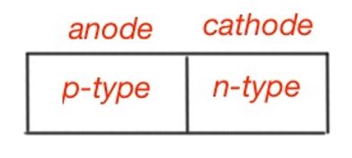
A junction of p-type and n-type semiconductors creates a diode. The p-type semiconductor acts as anode, the n-type as a cathode. If the voltage of the anode is bigger than the cathode voltage, then the diode is forward-biased and the current flows through the device. If the cathode voltage is bigger or equal to the anode voltage, then the diode is reverse-biased and there is a very small current that flows through the diode.
MOS (Metal-Oxide-Semiconductor) structure is similar to a sandwich and is created by the several layers of conducting and isolating materials. MOS structures are created by complex techniques, combining oxidation, doping, deposition and etching processes. Two types of transistors are produced by CMOS technology: an n-type transistor or nMOS and a p-type transistor or pMOS. Both these transistors are called MOSFETs (Metal Oxide Semiconductor Field Effect Transistor). Figure below depicts the scheme of a diode, Figure 2 shows schemes of n– and p-MOS transistors.
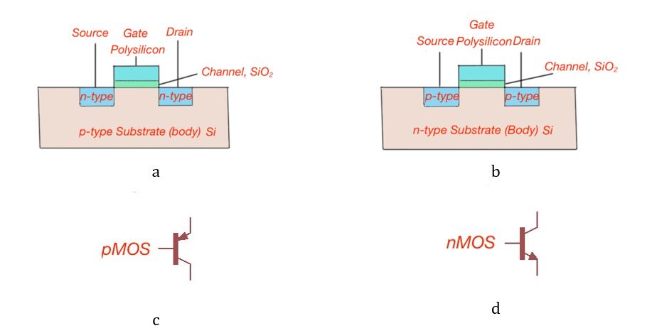
A transistor consists of a conducting gate, isolating the Si02 layer, and the silicon wafer, called a substrate. An n–MOS transistor consists of a p-type substrate, and n-type semicondutor – drain and source. A p–MOS transistor consists of an n-type substrate, and p-type drain and source.
Let’s consider how a transistor works. The gate is an input for any transistor. At the n–MOS transistor the substrate is grounded, so the p-n-junction of drain and source are reverse-biased. The transistor is off. When the gate voltage increases, the Si02 layer becomes the n-type semiconductor, and is called the channel – the current flows from source to drain. The transistor is on in this state.
At the p–MOS transistor, the substrate has a positive voltage. If the gate also has a positive voltage the transistor is off. If the gate voltage is lowered, positive charges the channel flow from the source to the drain. The transistor is on.
The positive voltage is called power and is marked as VDD, and represents logical 1 at digital circuits. It can have different voltage values, depending on the transistor. The lower voltage is called ground (GND) and is marked as VSS, and represented by logical 0 at the digital circuits. Figure 3 depicts p-and n-type transistors in operation.
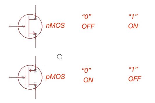
Figure 4 depicts the inverter scheme. The CMOS inverter is a combination p–MOS and n–MOS transistors as shown in the Figure 4. When the input I is given as 0, then the n–MOS transistor is off, and the p–MOS transistor is on. The output O has 1. When the input I is given as 1, then the p–MOS transistor is off, and the n–MOS transistor is ON, the output O has 0, as it is connected to the GND.
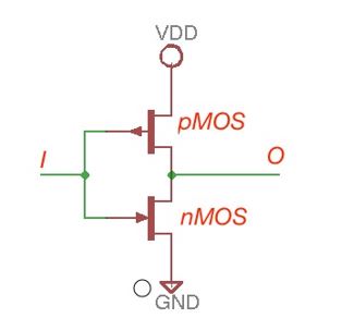
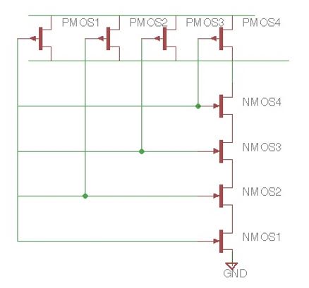
Figure 5 depicts the k-input NAND gate. The k-input NAND gate is a combination of k series n-MOS transistors between output and GND and k parallel p-MOS transistors between VDD and the output. When one of the inputs is 0, and the output is 1, when all the inputs are 1, the output is 0.
Educational content on VLSI topic can also be accessed via Reddit community r/ElectronicsEasy.

