This post covers CMOS device formation stepsCMOS processing is divided into two parts – FEOL (front-end-of-line) and BEOL (back-end of line). The CMOS device formation steps starts from wafer formation. Wafer is the thin disc of silicon, diced from the cylindrical boule of single-crystal silicon. This is the Czochralsky method for manufacturing of the single-crystal material.
The other process is photolitography, that defines areas of interest, using masks and photoresist. The wafers is subjected to the coting process with the photo resist and illumination process using photo mask. After the starting the initial process of photoresist coating, the other layers can be created, using masks. The mask is created with the chronium covered with the quartz glass. In order to expose the photoresist the ultraviolet source is used.
The photomask is called reticle, it is usually smaller then the wafer. The stepper is used to move the mask for photoresist exposing. The exposing process is called projection printing. The lightsource wavelength affect the geometrical characteristics of the . The lens system is used between the wafer and the mask. If we will define the minimum pitch (width+spacing) as . The is the numerical aperture, n is the refractive index of the lens, and is the lens characteristic.
The wavelength of the source comparable to the feature size create distortions in the pattern. In order to compensate the distortion the Resolution Enhancement Techniques are used (RET), that modify the wavelength, frequency and phase of the light. The light can be exposed on the wafer nonuniform, so the OPC (Optical Proximity Correction) method is used. It is used in order to avoid the undesired round corners. The phase shift mask (PSM) method is used to increase the desired grate. Off-axis illumination can as well be used to improve the contrast of the structure. The Double-patterning is the two precisely aligned exposure steps with different masks on the same photoresist layer.
For further creation of the semiconductor device the following techniques are used:
- N-well
- P-well
- Twin-well
- Triple-well
These processes were discussed before.
The important point of interest is silicon dioxide creation. The silicon dioxide can be used with the different thickness of the silicon dioxide layer for different devices, depending on the application. The thicker layers are needed for high voltage devices, The process of dioxide creation is called oxidation. Oxidation process happens in the oxidizing atmosphere after heating the silicon wafers. The most frequently used approaches are wet oxidation, dry oxidation and atomic layer deposition (ALD).
Another important process at the CMOS devices formation steps is the isolation. This process is used to separate the CMOS devices from one another. The n-well MOS or trench isolation is easy and quick way to isolate the noise-sensitive devices. The trench isolation also allows to place n-well and p-well devices closer together due to the higher drain/source breackdown voltage. The breakdown voltage is increasing with the depth of the trenches.
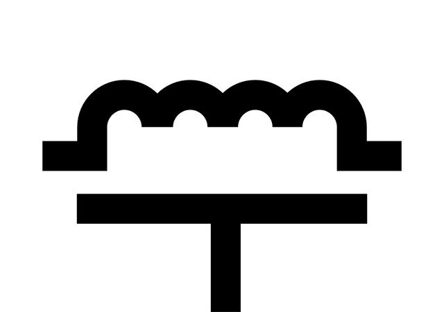
The other important step is gate oxide formation. Gate oxide usually places on the top of the planar structure. This structure is called the gate stack. The top oxide layer is preferably presented as the sequence of thin oxide layers, alternating with the nitride oxide layer, that decreasing the effective oxide thickness. The gate oxide formation is depicted on the Figure 1.
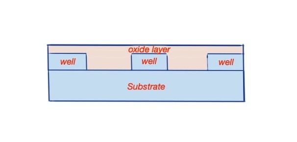
Figure 1. The gate oxide formation.
The next important step is the drain and source formation. Usually deposited silicon is a polysilicon layer. To improve the quality of the poysilicon is the annealing process is used. The annealing process is used to control the size of the single crystal domains, But undoped silicon has a very high resistivity. In order to decrease it the dopant implantation process can be used. This process is called self-aligned polysilicon gate process. It is consist of the few steps in order to define the drain, source and gate:
• To grow gate oxide layer for the transistor;
• Deposit polysilicon on chip;
• Pattern the polysilicon;
• Exposed gate oxide etching;
• nMOS/pMOS source/drain regions implantation.
The doping densities are in the range , which is relatively low. Schematically this process is depicted on the Figure 2.
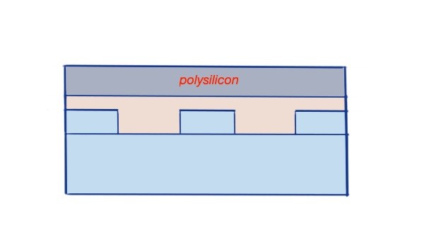
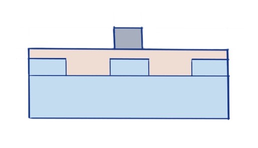
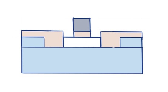
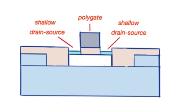
Figure 2. Gate and shallow source-drain creation process.
Contacts and metalisaion process is the on of the final processes of the CMOS formation. This process happens after the Gate/drain/source creation happens, and creates in the holes of the dielectric on the relevant regions. For the contacts formation can be used Al, Cu or W and other materials. The metalisation process is the process of wires creation between CMOS devices. The most used material for metalisation is aluminium. It is processed with the evaporation or sputtering process. After the evaporation process the dry or wet etching process is used to remove the unnecessary metal from the CMOS device surface.
The next step is passivation process. This is the process of adding the protecting glass layer that prevent the access for impurities. The passivation layer can also have the openings, that are used for the I/O pads access.
After the CMOS devise is created, the metrological research should be done. Large scale metrological research can be made with the optical microscopy. The small scale metrological research is done with the SEM (scanning electron microscopy) and TEM (transmission electron microscopy).
As mentioned previously, FEOL stands for Front End-Of-the-Line process. This process includes:
- Wafer material. Wafer material may vary depending on the application – it can be bulk Si, epi-layers, or SOI (silicon-on-isolator).
- STI (shallow trench isolation) is the most frequently used method of electrical isolation of CMOS devices.
- P-well and N-well formation;
- Gate formation;
- Drain/source formation;
BEOL stands for the Back End-Of-the-Line process, which includes:
- Self-aligned silicidation process;
- Pre-metal dielectric (the isolation between metal and silicon);
- Contact formation process (the electrical coupling between metal and polysilicon;
- Metalisation;
- Additional metal/dielectric layers;
- Passivation.
The back-end process then occurs. This includes the following processes:
- Wafer probe;
- Die separation;
- Packaging;
- Final tests.
Educational content can also be accessed via Reddit community r/ElectronicEasy.