
This post tells about power MOSFET characteristics and operating modes. Power MOSFET is a unipolar three-terminal semiconductor device that controls the large amounts of power flow between its input and output. Due to its low power dissipation, the efficiency of the device is very high, and that is significant in terms of the power dissipation level and the efficiency of the full system.
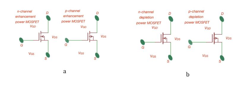
Power MOSFETs are more complex devices than low power MOSFETs, as they differ in structure, driver design and operational characteristics. Like low power MOSFETs, power MOSFETs can be divided into p- and n-types, enhancement and depletion MOSFETs. Power MOSFETs belong to a group of voltage controlled devices. That is the main difference between Power MOSFETs and BJTs.
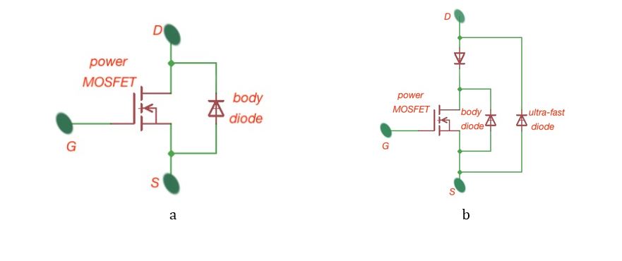
Power MOSFETs are characterised by the vertical structure that contributes to the increase the power ratio. Power MOSFETs usually contain a body diode in its structure, which is connected to the drain and source. This device makes bi-directional switch operation possible and enables reverse drain current. For some special applications designers put in a circuit diode, which blocks the body diode, and then add an external ultra-fast diode – Figure 2.
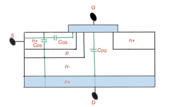
The power MOSFET also contains parasitic capacitances between terminals, that significantly influences the operation of devices. The capacitances are called gate-to-source capacitance, gate-to-drain capacitance and drain-to-source capacitance .
These capacitances have non-linear behaviour, and they depend significantly on device geometry, structure and biase volatges. Physically they are represented in Figure 3. Datasheets usually contain information about parasitic capacitances and body diodes. The datasheet capacitances have the following meanings: – small-signal reverse transfer capacitance, is small-signal capacitance when the drain and source terminals are shorted, is a small-signal capacitance when the gate and source terminals are shortened.
So the following formulas are valid: . As you can see, the MOSFET capacitances are the subject of voltage variation. In order for the MOSFET to start operating, capacitances and should be charged. The reason why the MOSFET operates with the drive circuit is because it charges and discharges the MOSFET parasitic capacitances to turn it on and off.
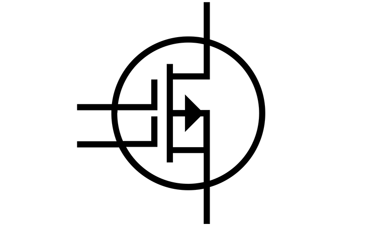
The most used type of power MOSFET is n-channel MOSFETs, enhanced-type. In order for the MOSFET to carry the drain current, there should be a drain to source channel. It may happen that the , the gate-source voltage of the MOSFET, exceeds the threshold voltage of the device .
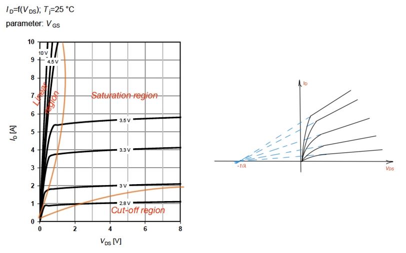
When , the MOSFET can be in stauration or in a linear region. When is small the device operates in a linear mode. When is large (), the device operates in a saturation regime. For the , then the device is in the cut-off region.
For all these regions the gate current is almost zero, it means that the device is voltage controlled. It is important to understand and distinguish these regions, because operation function of MOSFETs differ depending on operating regions. When a power MOSFET is used as an amplifier, it operates in its saturation region. When the power MOSFET is used as a switch, it operates in the cut-off and linear regions. Mathematically these regions can be expressed:
- Cut-off region ;
- Linear region
- Saturation region .
Here as you know µn is an electron mobility, is an oxide capacitance, L and W are the length and width of the channel.
As we know, when the power MOSFET enters the mode, when the channel is pinched-off, , then the saturation MOSFET mode can commence. We can prolong the curves on the output power MOSFET characteristics to the left as shown in Figure 4, and find an interception point of these curves – here is the positive constant MOSFET parameter. For example, Digi-Key Electronics offers a big selection of power MOSFETs.
(“Power Electronics Handbook”, 3rd edition, M.H. Rashid.; BSR606N, datasheet, Infineon Technologies AG).


