
This post gives an introduction into static induction transistors. Static induction devices (SID) are transistors operating with a prepunch-through region. These devices feature outstanding operating characteristics, with frequencies up to 1THz, and have great switching speed, low switching energy, large reverse voltage and low forward voltage drop.
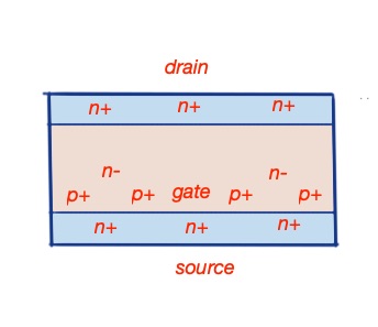
The potential along the static induction transistor channel and across the transistor channel can be described relatively with the function of the second order. , and for two channel dimensions, here is the height of the potential barrier. The drain current through the transistor will be . Here is the concentration of the source, are the geometrical characteristics of the potential saddle of the barrier. Here the potential is always a function of the gate and drain voltages.
Currents in the static induction transistors are controlled with the other characteristics – the space charge of the charge carriers.
SITs can be used to obtain the SID. These diodes have a low forward voltage drop. This diode can be made by shortening the emitter to the gate of the SIT (Figure 2).
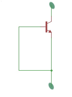
Figure 2.