AC coupling
The purpose of this activity is to investigate ac coupling and the use of a diode as a dc restoration circuit. Many signals contain a dc component. Often this dc must be removed and perhaps restored to a different dc level later in the signal path.
Written by Antoniu Miclaus and Doug Mercer of Analog Devices
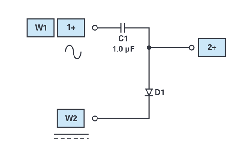
Set up the breadboard with W1 attached to one end of the 1.0 μF capacitor, as shown in Figure 18. The diode (D1) is connected between the other end of the 1.0 μF capacitor and the output of the second waveform generator, W2. The single-ended input of Scope Channel 2 (2+) is connected to the common connection of the capacitor and the diode.

Figure 18. Connection diagram for dc restoration circuit.
The first waveform generator should be configured for a 1 kHz sine wave with 2 V amplitude and 0 V offset to start. The offset will be varied and the effect on the output observed. The second waveform generator should be configured with 0 V amplitude and 0 V offset to start. The offset will be varied and the effect on the output observed. Scope Channel 2 (2+) is used to measure the voltage and should be set to 500 mV/div.
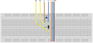
Figure 19. DC restoration breadboard circuit.
Plot the two waveforms using the oscilloscope provided by the Scopy tool.
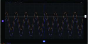
Figure 20. DC restoration waveforms.
Replace diode D1 in the circuit with a 10 kΩ resistor. Using the measurement tab on the scope, read and record the positive and negative peak values and mean value of Channel 2 (2+) as the offset of Waveform Generator channel 1 is changed between –1 and +1 volt. Now set Waveform Generator channel 1 to a square wave again with 2 V amplitude value. As done before, read and record the positive and negative peak values and the mean value as the duty cycle of the square wave is changed between 10% and 90%. Now remove the 10 kΩ resistor and put diode D1 back in place. Repeat the same measurements, adjusting the dc offset and duty cycle, that were just taken with resistor. How do they compare? Reverse the direction of diode D1 and again repeat these same measurements. How do they compare to the previous two?
Questions
What happened when the direction of D1 was reversed? What is the effect of setting different dc values for the output of Generator 2 (W2)?
Variable attenuator
The goal of this activity is to build, characterize, and analyse a small signal variable attenuator using a diode.
Set up the breadboard with the first waveform generator attached to one end of the 0.1 μF capacitor, as shown in Figure 22. Resistor R1 is connected between the second end of C1 and the junction of D1, R2, and C2. The other end of D1 is connected to ground. The second end of resistor R2 is connected to the wiper of the potentiometer R3. The ends of R3 are connected to ground and Vp (5 V) respectively. Scope Channel 2 (2+) is connected to the common connection of capacitor C2 and load resistor R4.
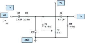
Figure 21. Connection diagram for variable attenuator.
Waveform generator W1 should be configured for a 10 kHz sine wave with 200 mV amplitude (or less) and offset set to 0. Set Scope Channel 1+ at 100 mV per division and Scope Channel 2+ connected at R4 to 100 mV per division. Set the measurements tab to display Ch1 peak-to-peak and Ch2 peak-to-peak.
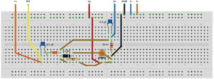
Figure 22. Variable attenuator breadboard circuit.
Plot the two waveforms using the oscilloscope provided by the Scopy tool.
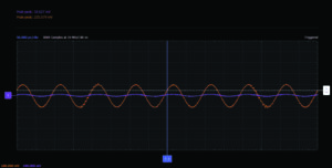
Figure 23. Variable attenuator waveforms.
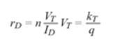
The purpose of C1 (and C2) is to block dc from the input and output circuits so that the operating point of the diode is not affected. The attenuator uses the fact that that small signal resistance of the diode rD is a function the dc flowing in the diode ID. See Equation below.
Where:
n is the diode area (size) scale factor VT is the thermal voltage
ID is the diode current
k is Boltzmann’s constant q is the electron charge
T is the absolute temperature
In the circuit, a voltage divider is set up between R1 and the resistance of D1. The current in D1 is varied by changing the current in R2. When the current in D1 is small, rD is large and the fraction of the input signal seen at the output is large. As the current in D1 increases, its resistance decreases, and the fraction of the input seen at the output decreases.
Questions
What is the maximum input signal level that you can use without distorting the output signal? What circuit parameter determines the upper limit of the input signal?
You can find the answers at the StudentZone blog, as well as further information on the topic. View the previous and next posts in this section on diodes.