Let’s continue with the seventeenth part in the series with an introduction to op amp configurations.
Written by Doug Mercer and Antoniu Miclaus
Objective:
In this lab, we will introduce the operational amplifier (op amp), an active circuit that is designed with certain characteristics (high input resistance, low output resistance, and a large differential gain) that make it a nearly ideal amplifier and useful building-block in many circuit applications. In this lab, you will learn about dc biasing for active circuits and explore a few of the basic functional op amp circuits. We will also use this lab to continue developing skills with the lab hardware.
Materials:
- ADALM1000 hardware module
- Solder-less breadboard and jumper wire kit
- One 1 kΩ resistor
- Three 4.7 kΩ resistors
- Two 10 kΩ resistors
- One 20 kΩ resistor
- Two AD8541 devices (CMOS rail-to-rail amplifier)
- Two 0.1 μΩ capacitors (radial lead)
1.1 Op amp basics
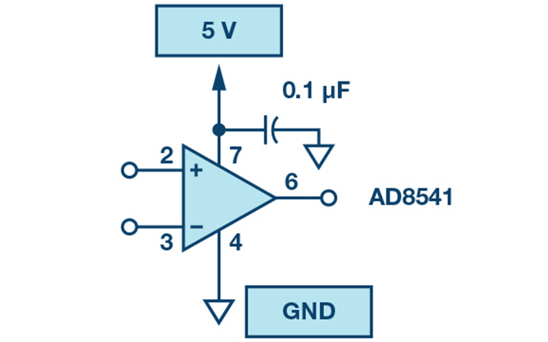
First step: connecting DC power
Op amps must always be supplied with dc power; therefore, it is best to configure these connections before adding any other circuit components. Figure 1 shows one possible power arrangement on your solder-less breadboard. We use two of the long rails for the positive supply voltage and ground, and one for 2.5 V mid-supply connections that may be required. Included are the so-called supply decoupling capacitors connected between the power supply and ground (GND) rails. It is too early to discuss in detail the purpose of these capacitors, but they are used to reduce noise on the supply lines and avoid parasitic oscillations. It is considered good practice in analogue circuit design to always include small bypass capacitors close to the supply pins of each op amp in your circuit.
Insert the op amp into your breadboard and add the wires and supply capacitors as shown in Figure 1. To avoid problems later, you may want to attach a small label to the breadboard to indicate which rails correspond to 5V, 2.5V, and ground. Colour code your wires: red for 5V, black for 2.5V, and green for GND. This can help to keep the connections organised.
Next, attach the 5V supply and GND connections from the ADALM1000 board to the terminals on your breadboard. Use jumper wires to power the rails. Remember, the power supply GND terminal will be our circuit ground reference. Once you have your supply connections you may want to use a DMM to probe the IC pins directly to ensure that pin 7 is at 5V and pin 4 is at 0V (ground).
Remember that you must have the ADALM1000 plugged into the USB port before measuring the voltages with the voltmeter.
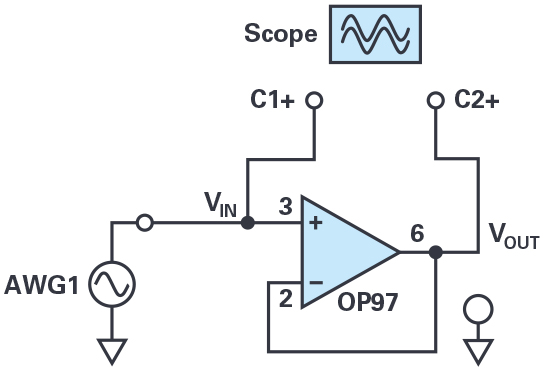
Unity-gain amplifier (Voltage follower):
Our first op amp circuit is a simple one (shown in Figure 2). This is called a unity-gain buffer, or sometimes just a voltage follower, and it is defined by the transfer function VOUT = VIN. At first glance it may seem like a useless device but, as we will show later, it finds use because of its high input resistance and low output resistance.
Using your breadboard and the ADALM1000 power supplies, construct the circuit shown in Figure 2. Note that the power connections have not been explicitly shown here; it is assumed that those connections must be made in any real circuit (as you did in the previous step), so it is unnecessary to show them in the schematic from this point on. Use jumper wires to connect input and output to the waveform generator output, CA-V, and oscilloscope input, CB-H.
Use the Channel A voltage generator set to a 1.0V min value and a 4.0V max value (3V p-p centered on 2.5V), with a 500Hz sine wave. Configure the scope so that the input signal trace is displayed as CA-V and the output signal trace is displayed as CB-V. Export a plot of the two resulting waveforms and include it your lab report, noting the parameters of the waveforms (peak values and the fundamental time period or frequency). Your waveforms should confirm the description of this as a unity-gain or voltage follower circuit.
Buffering example:
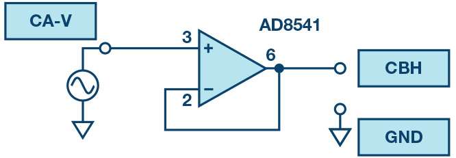
The high input resistance of the op amp (zero input current) means there is very little loading on the generator; that is, no current is drawn from the source circuit and therefore no voltage drops on any internal resistance (Thevenin equivalent). Thus, in this configuration the op amp acts like a buffer to shield the source from the loading effects from other parts of the system. From the perspective of the load circuit, the buffer transforms a nonideal voltage source into a nearly ideal source. Figure 3 describes a simple circuit that we can use to demonstrate this feature of a unity-gain buffer. Here the buffer is inserted between a voltage-divider circuit and some load resistance, the 10kΩ resistor.
Disconnect the power supplies and add the resistors to your circuit as shown in Figure 3 (note that we have not changed the op amp connections here, we’ve just flipped the op amp symbol relative to Figure 2 to better arrange the wires).
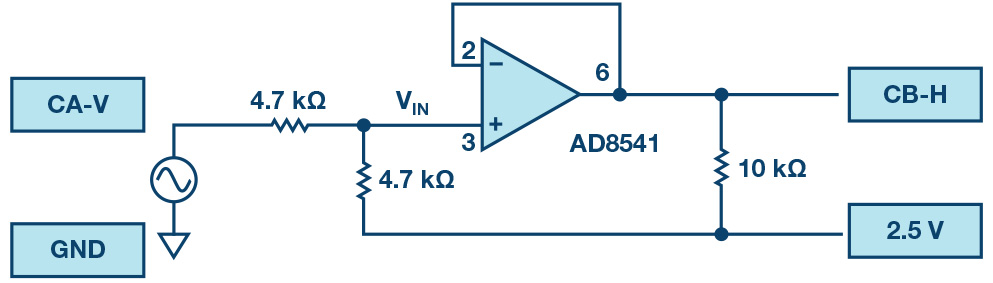
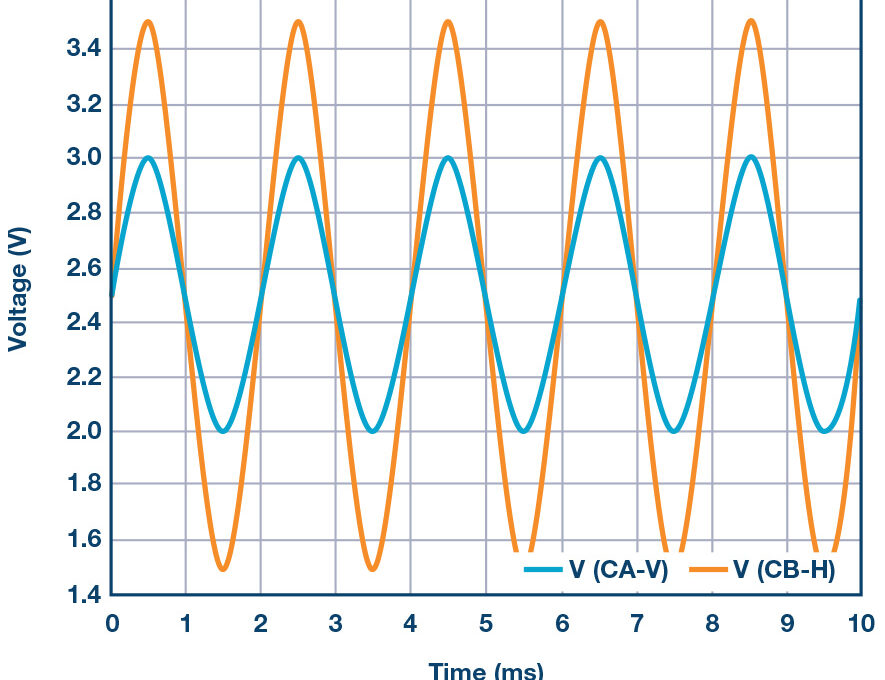
Reconnect the power supplies and set the waveform generator to a 500Hz sine wave set to a 0.5V min value and a 4.5V max value (4V p-p centred on 2.5V). Simultaneously observe VIN CA-V and VOUT CB-H and record the amplitudes in your lab report. Use scope input CB-H to also measure the amplitude of the signal seen on pin 3 of the op amp.
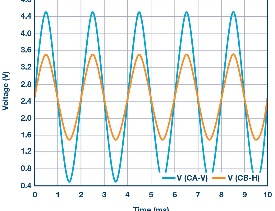
A plot example is presented in Figure 4.
Remove the 10 kΩ load and substitute a 1kΩ resistor instead. Record the amplitude. Now move the 1kΩ load between pin 3 and 2.5V, so that it is in parallel with the 4.7kΩ resistor. Record how the output amplitude has changed. Can you predict the new output amplitude?
Simple amplifier configurations
Inverting amplifier:
Now assemble the inverting amplifier circuit shown in Figure 5 using R2 = 4.7kΩ. Remember to disconnect the power supply before assembling a new circuit. Cut and bend the resistor leads as needed to keep them flat against the board surface and use the shortest jumper wires for each connection (as in Figure 1). Remember, the breadboard gives you a lot of flexibility. For example, the leads of resistor R2 do not necessarily have to bridge over the op amp from pin 2 to pin 6; you could use an intermediate node and a jumper wire to go around the device instead.
Reconnect the power supplies and observe the current draw to be sure there are no accidental shorts. Now adjust the waveform generator to a 500Hz sine wave set to a 2.1V min value and a 2.9V max value (0.8V p-p centred on 2.5 V) and again display both the input and output on the oscilloscope. Measure and record the voltage gain of this circuit and compare to the theory that was discussed in class. Export a plot of the input/ output waveforms to be included your lab report.
A plot example is presented in Figure 6.
This is a good point to comment on circuit debugging. At some point in your classes, you are likely to have trouble getting your circuit to work. That is not unexpected, nobody is perfect. However, you should not simply assume that a non-functional circuit must imply a malfunctioning part or lab instrument. That is almost never true; 99% of all circuit problems are simple wiring or power supply errors. Even experienced engineers will make mistakes from time to time, and, consequently, learning how to debug circuit problems is a very important part of the learning process.
It is not the TA’s responsibility to diagnose errors for you, and if you find yourself relying on others in this way, then you are missing a key point of the lab and you will be unlikely to succeed in later coursework. Unless smoke is issuing from your op amp there are brown burn marks on your resistors, or your capacitor has exploded, your components are probably fine. In fact, most of them can tolerate a little abuse before significant damage is done. The best thing to do when things aren’t working is to just disconnect the power supplies and look for a simple explanation before blaming parts or equipment. The DMM can be a valuable debugging tool in this regard.
Output saturation:
Now change the feedback resistor R2 in Figure 5 from 4.7kΩ to 10kΩ. What is the gain now? Slowly increase the amplitude of the input signal to 2V still centered on 2.5V and export the waveforms into your lab notebook. The output voltage of any op amp is ultimately limited by the supply voltages, and in many cases the actual limits are much smaller than the supply voltages due to internal voltage drops in the circuitry. Quantify the internal voltage drops in the AD8541 based on your measurements above. If you have time, try substituting an OP97 or OP27 amplifier for the AD8541 and compare the minimum and maximum output voltages that it can produce.
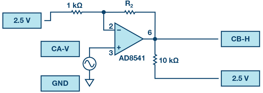
Summing amplifier circuit:
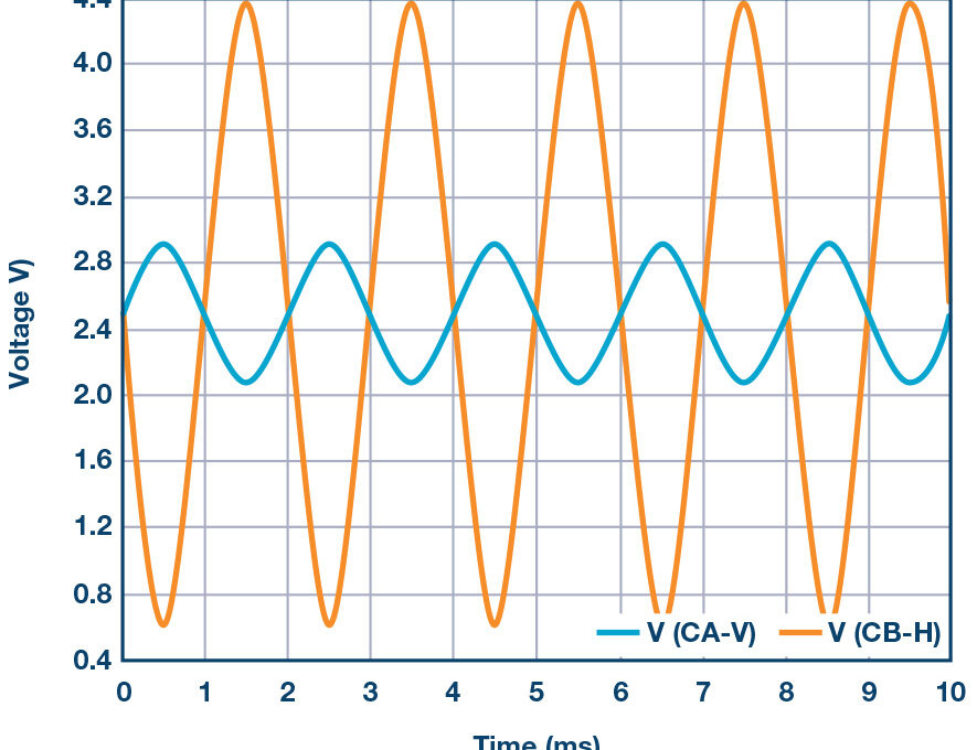
The circuit of Figure 7 is a basic inverting amplifier with four inputs, called a summing amplifier. Figure 7 is configured slightly differently than you may see in text books because of the single positive supply voltage available from the ADALM1000. The noninverting (+) input of the amplifier is connected to 2.5V, which is half the supply voltage, rather than ground. This changes the summing amplifier equations. The input voltages, which appear across the input resistors, now are taken with respect to the 2.5V so called common-mode level. They should have the 2.5V subtracted, so 0VIN becomes –2.5V and +3.3VIN becomes +0.8V.
The output voltage should also be taken with respect to the +2.5V level. To make the conventional equation come out right, the output voltage will also have the 2.5V common-mode level subtracted. Another way to think about this is to consider the case where all the inputs are at 2.5V (or are left floating). There will be no current flowing in any of the input resistors (they have 0 V across them) and as a result the feedback resistor will also have no current flowing in it (it has 0 V across it). The output will be at 2.5V.
For this circuit you will be using the four digital outputs, PIO 0, PIO 1, PIO 2, and PIO 3, as input voltage sources. Each digital output has either a low output near 0V or a high output near 3.3 V. Using superposition (and correcting for the 2.5 V common-mode level) we can show that VOUT is a linear sum of VPIO0, VPIO1, VPIO2, and VPIO3, each with their own unique gain or scale factor set by the ratio of the 1 kΩ feedback resistor divided by their respective resistors.
PIO 0 has the highest value and will have the smallest change in the output (least significant bit) and PIO 3 has the lowest value and will have the largest change in the output (most significant bit). Notice that the PIO 3 resistor is made from 2 × 4.7kΩ resistors in parallel.
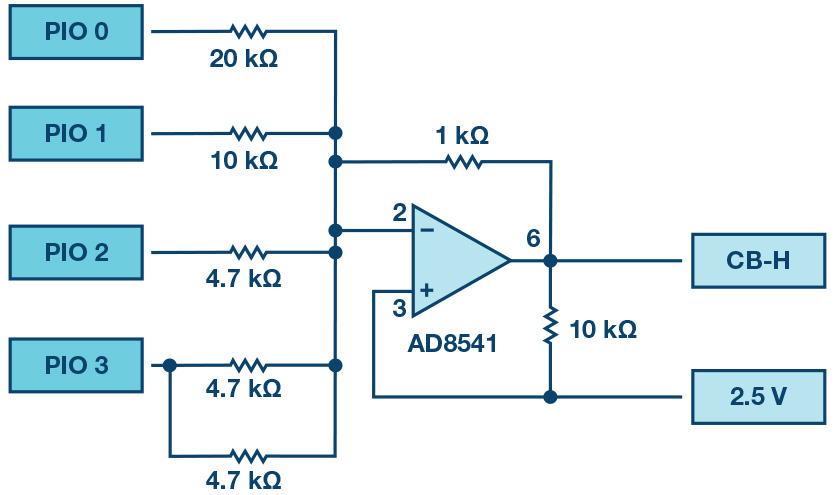
With the power disconnected, modify your inverting amplifier circuit as shown in Figure 7. Reconnect the power and, using the digital output controls, fill in the following two tables. In the first table, record the low and high voltages for each digital output. Use the CB-H scope input in high-Z mode to do this. In the second table, record the output voltage for all 16 combinations of 1s and 0s for PIO 0, PIO 1, PIO 2, and PIO 3. You should also confirm that the output voltage is indeed 2.5V when all four bits are floating or in the high-z (X) state.
Table 1. Low and high voltages
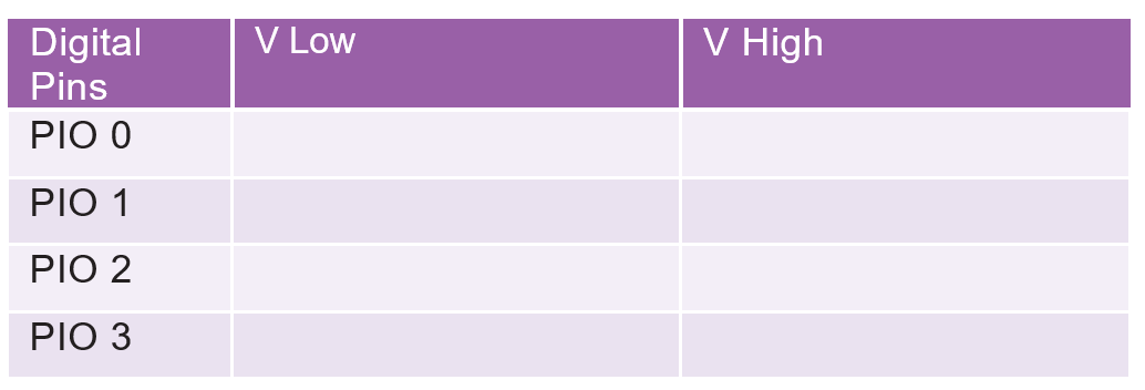
Table 2. Output voltage
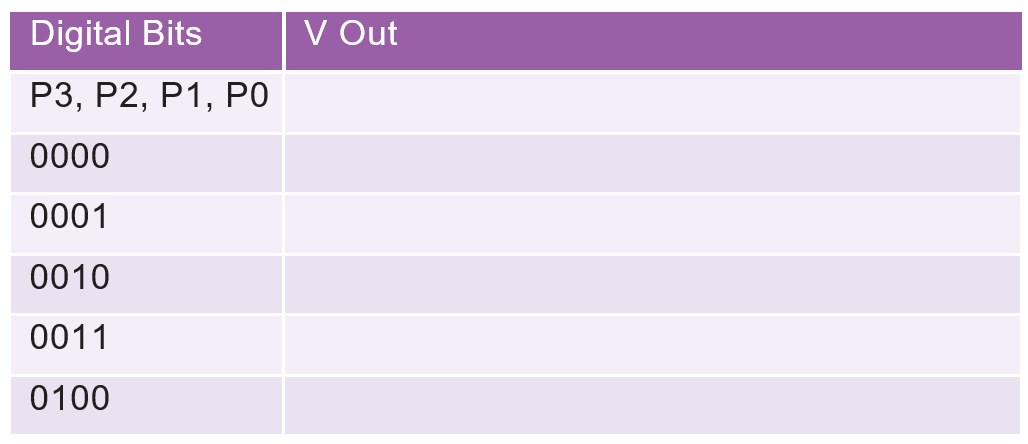
Using the resistor values, calculate the expected output voltage for each input combination and compare to your measured values.
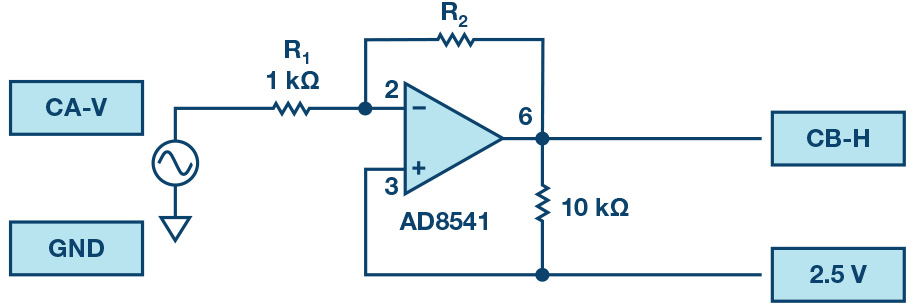
Assemble the noninverting amplifier circuit shown in Figure 8. Remember to shut off the power supplies before assembling the new circuit. Start with R2 = 1kΩ.
Apply a 500Hz sine wave from CA-V set to a 2.0V min value and a 3.0V max value (1 V p-p centered on 2.5V) and display both input and output waveforms on the scope. Measure the voltage gain of this circuit and compare to the theory discussed in class. Export a plot of the waveforms and include it in your lab report.
A plot example is presented in Figure 9.
Increase the feedback resistor (R2) from 1kΩ to about 4.7kΩ. Remember you may need to reduce the amplitude of the input to prevent the output from saturating (clipping). What is the gain now?
Increase the feedback resistance until the onset of clipping—that is, until the peaks of the output signal begin to be flattened due to output saturation. Record the value of resistance where this happens. Now increase the feedback resistance to 100kΩ. Describe and draw waveforms in your notebook. What is the theoretical gain at this point? How small would the input signal have to be in order to keep the output level to less than 5V given this gain? Try to adjust the waveform generator to this value. Describe the output achieved.
The last step underscores an important consideration for high gain amplifiers. High gain necessarily implies a large output for a small input level. Sometimes this can lead to inadvertent saturation due to the amplification of some low-level noise or interference, for example, the amplification of stray 60Hz signals from power-lines that can sometimes be picked up. Amplifiers will amplify any signals at the input terminals … whether you want it or not!
Using an op amp as a comparator
The high intrinsic gain of the op amp and the output saturation effects can be exploited by configuring the op amp as a comparator, as shown in Figure 10. This is essentially a binary state, decision-making circuit: If the voltage at the “+” terminal is greater than the voltage at the “–” terminal, VIN > VREF, the output goes high (saturates at its maximum value). Conversely, if VIN < VREF, the output goes low. The circuit compares the voltages at the two inputs and generates an output based on the relative values. Unlike all the previous circuits there is no feedback between the input and output; when this happens, we say that the circuit is operating open loop.
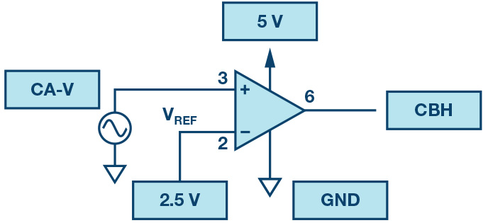
Comparators are used in different ways and in future sections we will see them in action. Here we will use the comparator in a common configuration that generates a square wave with a variable pulse width. Start by disconnecting the power supplies and assemble the circuit. Use the fixed 2.5V output for the dc source on the inverting input, VREF.
Again, configure the waveform generator CA-V on the noninverting input, for a 2V min value and 3V max value triangle wave (centred on 2.5V) at 500Hz. With the power supply reconnected, export the input and output waveforms.
A plot example is presented in Figure 11.
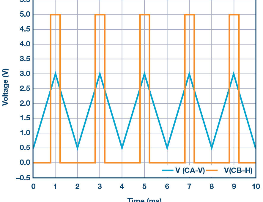
Now slowly shift the center of the triangle wave by increasing (positive shift) or decreasing (negative shift) the minimum and maximum values and observe what happens at the output. Can you explain this?
Repeat the above for a sine wave and sawtooth input waveforms and record your observations for your lab report.
Questions
- Slew rate: how do you measure and compute the slew rate in the unity-gain buffer configuration? Compare this with the value listed in the OP97 data sheet.
- Summing circuit: using superposition, derive the expected transfer characteristic for the circuit of Figure 8. Find the output voltage in terms of VIN0, VIN1, VIN2, and VIN3. Compare the predictions of the ideal relationship with your data.
- Comparator: what would happen if the polarity of VREF is reversed?
You can find the answers at the StudentZone blog.