Written by Antoniu Miclaus and Doug Mercer of Analog Devices
Absolute value circuits
The purpose of this activity is to investigate absolute value circuits. Rectifiers, or absolute value circuits, are often used as detectors to convert the amplitudes of ac signals to dc values to be more easily measured. For this type of circuit, the ac signal is first high-pass filtered to remove any dc term, then rectified and perhaps low-pass filtered. As we have seen in the simple rectifier circuits constructed with diodes, the circuit does not respond well to signals with a magnitude less than a diode drop (0.6 V for silicon diodes). This limits their use in designs where small amplitudes are to be measured. For designs in which a high degree of precision is needed, op amps can be used in conjunction with diodes to build precision rectifiers.
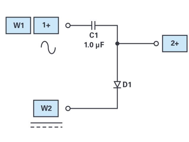
The inverting op amp circuit can be converted into an ideal (linear precision) half-wave rectifier by adding two diodes, as shown in Figure 24. For the negative half of the input diode, D1 is reverse biased and diode D2 is forward biased and the circuit operates as a conventional inverter with a gain of –1. For the positive half of the input, diode D1 is forward biased, closing the feedback around the amplifier. Diode D2 is reverse biased disconnecting the output from the amplifier. The output will be at the virtual ground potential (–input terminal) through the 10 kΩ resistor.
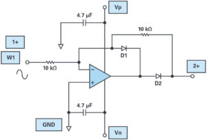
Figure 24. Connection diagram for a precision half-wave rectifier.
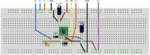
Figure 25. Precision half-wave rectifier breadboard circuit.
The peak of the rectified output, as seen in Figure 26, is now equal to the peak value of the input. There is also a sharp transition as the input crosses zero. The experimenter should investigate the waveforms at different points in the circuit to explain why this circuit works better than the simple diode half-wave rectifier.
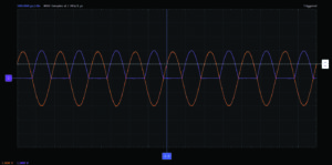
Figure 26. Precision half-wave rectifier waveforms.
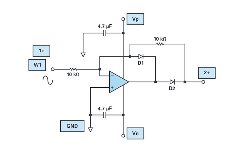
The circuit shown in Figure 27 is an absolute value circuit, often called a precision full-wave rectifier. It should operate like a full-wave rectifier circuit constructed with ideal diodes (the voltage across the diode, in forward conduction, equals 0 V). The actual diodes used in the circuit will have a forward voltage of around 0.6 V.
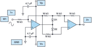
Figure 27. Connection diagram for absolute value circuit.
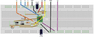
Figure 28. Absolute value breadboard circuit.
Things to consider
- Study the circuit and determine how it works. There is very fundamental concept that should help in understanding how this circuit operates. Given an op amp configured with negative feedback, the inverting and noninverting input terminals will try to reach the same voltage level, often referred to as a virtual short.
- Plan some tests to see if this circuit indeed is an absolute value circuit. Perform these tests, fully documenting all tests and results.
- Make the input voltage a 6 V amplitude sinusoid at 1 kHz. Carefully measure and record voltages at all nodes in the circuit.
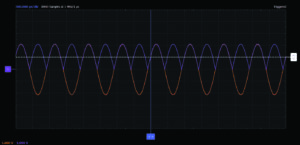
Figure 29. Absolute value waveforms.
Questions
Report on your experiments by fully documenting all tests and results.
Voltage doubler circuits
Voltage doublers are very useful in situations where the load current is relatively light, and the required dc voltage is higher than what is available from the system power supply.
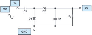
Figure 30. Connection diagram for voltage doubler circuit.
How this circuit operates is not as straightforward as the diode rectifier circuits we examined earlier. To understand this circuit, we need to look at it during successive half-cycles of the ac input from W1. We will start by assuming ideal components and that C1 = C2.
- During the first negative half-cycle, D1 will be forward biased and will hold the right end of C1 at one diode drop below ground. Therefore, C1 will charge to a voltage nearly equal to the peak voltage (vPEAK) of the ac input, with its left end being negative with respect to ground.
- During the following positive half cycle, D1 will be reverse biased and will not conduct current. The voltage on C1 will add to the ac input voltage, so a voltage of approximately 2 VPEAK will appear at the left end of D2. Since C2 is not yet charged at all, this will forward bias D2 and allow the voltage at the right end of C1 to be applied to the top of C2. C2 will charge as C1 discharges, until the two capacitors can no longer forward bias D2. For the first positive half-cycle, the voltage on C2 will be equal to VPEAK, and C1 will be completely discharged, so that all the voltage at the left end of D2 comes from the ac input.
- On the next negative half-cycle, C1 charges again to VPEAK, through D1. If there is no load to discharge C2, its output will remain at +VPEAK.
- On the second positive half-cycle, C2 is still charged to +VPEAK, while the voltage at the left end of D2 is again +2 VPEAK. Again, C1 transfers part of its charge to C2, but this time they stop when C2 is charged to a voltage of +1.5 VPEAK.
- This action continues, cycle by cycle, with C1 being fully recharged to VPEAK on each negative half cycle, and then charging C2 to a voltage halfway between its starting voltage and +2 VPEAK. C2 will never quite charge to +2 VPEAK, but it will come very close.
With nonideal components there is a small (0.6) voltage drop across each diode when it is forward biased. This will reduce the maximum no load output voltage of the doubler. Any load on this circuit, such as RL, will always draw current from C2, thus discharging this capacitor to some extent. On each positive half-cycle, C1 will recharge C2 from the voltage it had at the start of the half-cycle halfway up to +2 VPEAK. The ripple on the output will be larger and the average dc value will be lower.
Note that the output current capacity of this circuit is only half the current capacity of a normal rectifier circuit. Any additional load current taken from the voltage doubler will simply cause C2 to discharge faster, thus reducing the output voltage. It is never possible to get more power out of the voltage doubler than goes into it.
The charging and recharging of C2 can be made faster if C1 is made larger than C2. For example, if C1 = 10 µF and C2 = 1 µF, C1 can transfer much more charge to C2 on each positive half-cycle, and the voltage on C2 will increase much faster than the voltage on C1 will decrease. Of course, this also means that the output current capacity is even more limited, since C2 will discharge rapidly as well as charge rapidly.
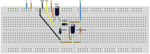
Figure 31. Voltage doubler breadboard circuit.
Finally, plot the two waveforms using the oscilloscope provided by the Scopy tool.
Questions
The circuit in Figure 30 produces a positive dc output voltage. How can it be reconfigured to make a negative output voltage? Construct the voltage inverter and repeat the experiment/simulation.
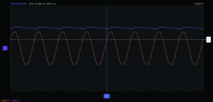
Figure 32. Voltage doubler waveforms.
You can find the answers at the StudentZone blog, as well as further information on the topic. View the previous post in this section on diodes.