The power BJT static characteristics determine the safe operational regime of the device. These characteristics are usually described in the datasheet as maximum ratings. This data is calculated, not measured. It is made for the designer to use the power BJT in a safe mode, maintaining it’s reliability, avoiding failures due to the avalanche mechanisms, contacts evaporation and other degradation mechanisms.
For example, the static characteristics of the Toshiba npn power Bipolar Junction Transistor, 2SC5198 are mentioned in the table of maximum ratings, and are collector-base voltage, collector-emitter voltage, emitter-base voltage, collector and base current and power dissipation characteristics.
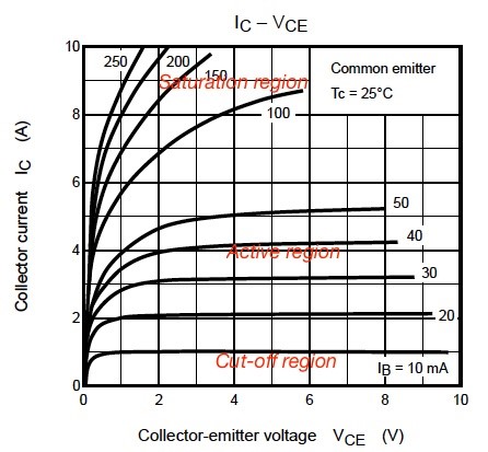
The datasheet also shows several curves like the current-voltage curves (collector current vs. collector-emitter voltage, collector current vs base-emitter voltage). Figure 1 shows the family of curves for the power BJT that indicate the operating regions of the BJT (saturation, active and cut-off region).
This curve vs is measured at a certain level of base current . The cut-off region occurs when the collector current is very close to zero and changes non–linearly. The saturation region commences when the collector-emitter voltage is less than the base voltage – this region is non–linear.
It is better not to use the device in this region. The third region here is active or linear, where the collector current is constant for different levels of current-emitter voltage VCE, i.e. the transistor acts like a current source. If we prolong the tangent to the curves to the left, they will finally cross and we will get the early voltage point. This parameter shows how close our transistor is to an ideal one.

The function of a collector current vs base-emitter voltage reminds the current-voltage characteristics of the diode. If we draw the reverse ratio, it will cross with the original curve in the operating point Q, which indicates the dynamic resistance.
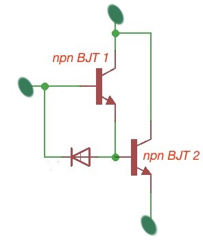
As the BJT may work in the regime of the current amplification, when the collector current is the function of the base curent, so the BJT may be useful for the Darlington scheme, where one transistor amplifies the current and another transistor amplifies the already amplified current. The Darlington scheme consists of two transistors and is depicted in Figure 2. If the and are the amplification parameters of transistors, then is the gain of the Darlington scheme.

When the current is very high at the BJT, there is a current-emitter voltage drop which may occur and lead to power dissipation problems. The heat is distributed across the transistor non-uniformely, so some parts of the semiconductuctor may overheat which will cause the semiconductor to melt, crack and result in failure.
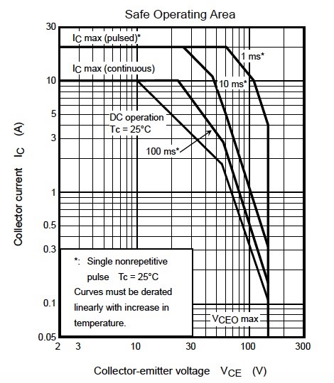
To avoide these effects it is better to keep the power dissipation of the device under control and keep the work parameters of the device inside the boundaries of Safe Operation Area (SOA), which is usually depicted in the datasheet.
The SOA curves show the maximum ratings of current, voltage and power dissipation for reliable usage of a transistor. The SOA curves also determine the peak power handling capability. It determines the ability of a BJT to switch high currents reliably without failures. We must note that current and thermal density are also important for reliable transistor operation, as there are overheating spots which may occur in the transistor, but when the power and heat are widely and uniformly distributed across the transistor, it will guarantee long and reliable transistor operation.
To calculate the power dissipation for a certain work regime of a BJT, it is good to use the formula . It is simple and helps the designer to quickly estimate if the current work regime corresponds to the transistor SOA. Figure 3 shows the SOA curves for the considered 2SC5198 transistor.

(The Power Electronics Handbook”, 3rd Edition, M.H. Rashid, Elsevier.; Toshiba NPN BJT transistor 2SC5198 datasheet).


