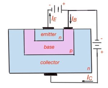
This post tells about characteristics of power BJT. Power BJT consists of three pieces – collector (C), emitter (E) and base (B). The size of the emitter-base junction is usually much smaller then the size of collector-base junction and the base thickness is usually also small.
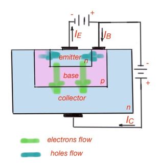
In our case, the base is a low-doped p-type semiconductor, which increases the resistance of p-type material. When the BE junction is forward-biased, electrons go from the emitter into the base.
As mentioned above, the base is thin and many of the electrons can cross it easily, reaching the collector region that forms the consistent of the electric charge carriers, so that the collector current is only slightly less than the emitter current.
The base-collector area is a reverse-biased junction, and there is a depletion region on the junction. When the electrons reach the base-collector junction and the depletion layer, the electric field pulls the electrons in the collector area.
So the amount of electrons go through the emitter and the amount of electrons that go through the collector appears more or less similar. The reverse-biased position of the collector makes the holes go from the base to the emitter and impacts on the current emitter-collector. The relationship between the emitter and the collector current (the last one as a result can be controlled by base voltage) is as follows:
The current flows through the BJT as depicted in Figure 2.
Here so , where .
The parameters χ and ζ are dependent on the characteristics of power BJT material, and the doping levels of the transitor n and p regions. There is a doping or drift layer added between the collector and the base, or between the metallisation and collector in order to increase the power dissipation in a device. This planar structure is also determined by a large breakdown voltage and large blocking voltage.1
Some BJTs are made with a Silicon Carbide (SiC) semiconductor. This material is very good for use in power and frequency applications. For example, Hyung-Seok Lee, in his thesis ‘High Power Bipolar Junction Transistors in SiC’ describes preparation of the BJT with p- and n-type SiC, 4H-SiC polytyp.
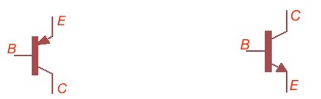
This polytyp has the widest bandgap across the most popular semiconductors for electronics like Si, GaAs, GaN, 3C-SiC, and 6H-SiC, and it is also characterised by high break-down electric field and thermal conductivity. This paper gives an extensive explanation of the growth processing for the SiC BJT, with the arguments for certain doping levels and metallisation materials, like Al- and Ni-based metallisation. The electrical symbols of BJT transistors are depicted in Figure 3.2
1 “Power Electronics Handbook”, Third Edition, M.H. Rashid, Elsevier, 2011.
2 “High Power Bipolar Junction Transistors on Silicon Carbide”, Licenciate Thesis, Hyung-Seok Lee, 2005.