This post answers the question “What is propagation delay in logic gates?”. Effects happening in the RC circuits are the source of the propagation delay in digital circuits.
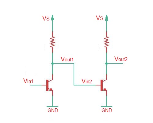
Let’s consider two inverters in series as depicted below.
In case of input step function, the voltage waveform at the output of the first MOSFET is depicted below. In order for signal get from state to state, there is a time interval , and then after the signal changes from the state to , it happens within the time interval .
Generally speaking the parameters and are called propagation delay of an inverter for the state or . These two delays are not always equal to each other, so for simplicity the propagation delay is usually chosen the biggest of them .
Lets consider general case of combinational digital circuit with multiple inputs and outputs. We can apply the terms of propagation delays mentioned above as follows:
is the signal propagation delay for selected input and output terminal for high to low instantaneous transition at the input. is the signal propagation delay for selected input and output terminal for low to high instantaneous transition at the input.So signal propagation delay for selected input-output terminals of combinational circuit is .
The output of combinational circuit is characterised with rise and fall times. Rise time of the output is the delay in rising from the lowest value valid high level of the signal at the output. Fall time of the output is the delay in falling from the highest value to the valid low value at the output.
It’s important to remember that the propagation delay and the rise/fall times are not equal.
Normally digital devices should interpret correctly voltages that belongs to the valid input thresholds, resulting the output values that belong to the valid output range. Due to RC effects the transition on the output goes slower.
Let’s get back again to the series connection of two inverters, presented in SRC model on the figure below. For the case of high input the first circuit works, for the case of low input the second circuit works.
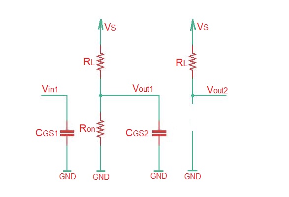
In order to calculate the magnitude of the propagation delay of MOSFET, we must consider it’s SRC model. Getting back to two inverters connected in series, that can be represented as depicted below.
When the signal is high, then SRC circuit model looks as depicted below. Here the second capacitor is an open circuit.
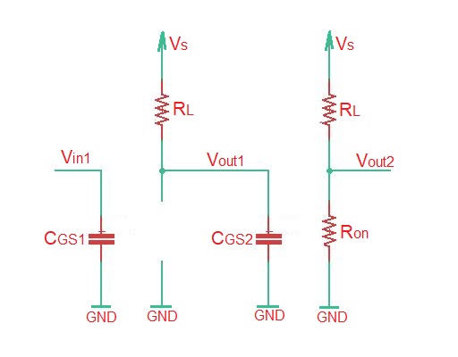
When signal is low, then SRC circuit model looks as depicted below. Here the second capacitor is charging.
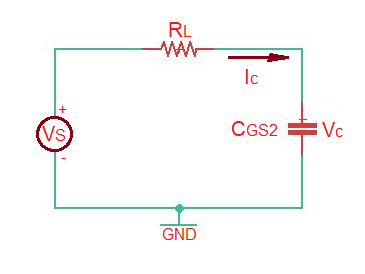
Let’s write down KCL for the circuit so . The solution of this differential equation is the sum of homogeneous and particular solutions .
When signal is high, then SRC circuit model looks as depicted below. Here the second capacitor is discharging.
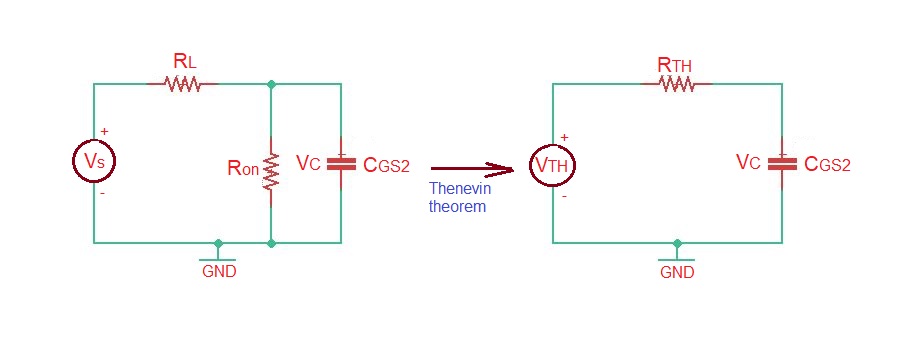
In accordance to Thenevin transformation we have and .
Building a KCL for the last circuit we are having a differential equation so .
The total solution of this differential equation is the sum homogeneous and particular solutions and we have .
The following parameters are known constants, calculating for different levels of we can find and delays, that will allow us to calculate the propagation delay .
Educational content can also be reached via Reddit community r/ElectronicsEasy.