As discussed above a half-wave rectifier is not the best AC-DC converter, because it does not conduct half of the wave. The full-wave rectifier is a much better option. The scheme of a half-wave rectifier is depicted in Figure 6 in a circuit with AC signal supply and load resistor. The first part of a full-wave rectifier includes the AC voltage supply, and transformer, characterised with 1:N ratio.
The transformer is needed to enlarge or decrease the voltage magnitude before rectification. The second part of a full-wave rectifier includes the diode. This scheme for a full-wave rectifier is characterised by the feature that the positive half-wave of the signal goes through the top diode, that is forward-biased, the negative half-wave of the signal goes through the bottom diode, reverse-biased. For the industrial electrical lines the offset voltage is very small and the diodes can be assumed as ideal ones. So, according to the scheme for a full-wave rectifier we get: .
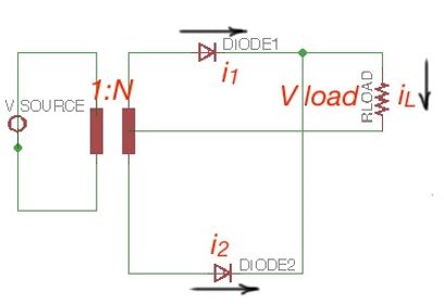
The full-wave rectifier is two-fold more efficient than a half-wave rectifier in this case. Another application of a diode is a bridge rectifier. The bridge is designed to conduct through the diodes and in the case of a positive half wave from the AC source; and through the diodes and for negative half-wave.
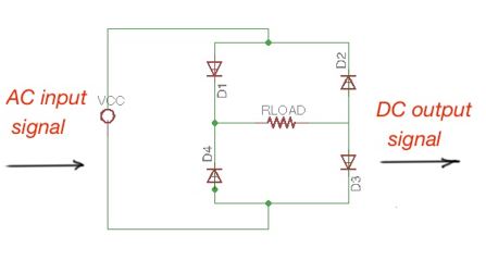
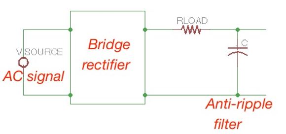
Conventional and bridge-rectifiers are properly transforming AC signals with zero average value to a non-zero DC signal. However, these signals are still an oscillating waveform. The result of this transformation is ripple. It means the rectifier is still generating the series of pulsed signals with bigger frequency than the former signal. To filter the average DC voltage from these signals a low-pass filter is needed.
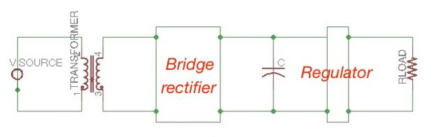
Power supplies and voltage regulation
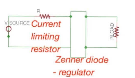
The rectification process described above is widely used. Functionally the schemes are called the DC power supply, because they are used in the process of extracting the DC signal from the former AC signal. After obtaining the DC signal, a DC voltage regulator is used in a circuit to avoid any possible fluctuations of voltage. The DC power supply scheme is depicted below as a block-diagram. The Zenner diode is usually used as a regulator in these schemes, due to its ability to maintain specific voltage level for the range of currents.
Zenner regulation for this scheme can be represented with the circuit in Figure 10. Remembering the features of the Zenner diode:
- If the , the diode operates as a short-cut;
- If , the diode operates as an open-circuit;
- If , the diode operates in a reverse-biased regime and can maintain a certain level of voltage.
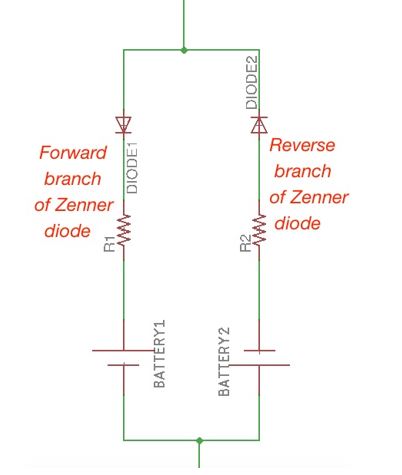
Here below is depicted how a Zenner diode operates as a voltage regulator. From this scheme we can see the main points of characterising a Zenner diode as a regulator:
The Zenner diode is characterised by its power dissipation ability . The load resistances, which can be applied in certain Zenner diodes, is limited by the range: where corresponds to the max source current, is related to the diode power dissipation.