Limiter
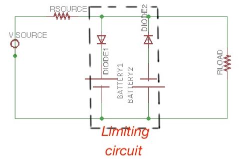
A limiter is a diode circuit that is designed to keep voltages at the load in a certain voltage range –, so the maximum dangerous voltage levels for a circuit will not be reached. It is obtained by cutting the initial AC signal to a certain level. Figure below depicts the scheme of the limiter with inverse parallel diodes. Here the diode cuts a positive peak, and diode cuts a negative peak of the initial circuit.
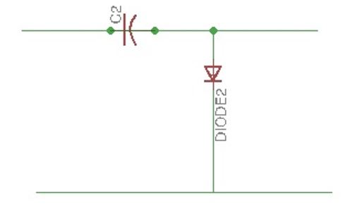
The clamp diode
The purpose of this diode is to clamp the AC signal to the DC value. The principal scheme of the clamp diode is depicted below. As long as the diode is conducting in the forward direction, the capacitor will charge only at the positive half-wave of the AC signal. The capacitor will charge until the value , of the capacitor is shifted to .
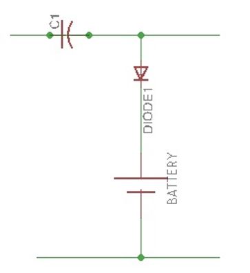
The positive peaks are now shifted, and it is important that the where is a period of the signal. Figure below depicts the AC signal in the initial state and is clamped. The clamp diode can also work in the reverse direction, and the capacitor will charge to the voltage -, and the output voltage will be . Negative voltage peaks will be shifted to 0V, as all the graphs will be moved to . The signal clamp can also be made by using a battery , where . This circuit is called the biased diode clamp.
Photodiodes
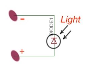
Semiconductor diodes can also be useful because of their ability to react on the light energy, when the light photons are reaching the depletion region, they stimulate the hole-electron generation process, which is called photo-ionisation. The top-material is transparent. The reverse saturation current is dependent on the light intensity, where is a current caused by photo-ionisation. The characteristics for this diode are depicted below, and it is shifted down to the value of , and also we can see the diode operation points for each diode.
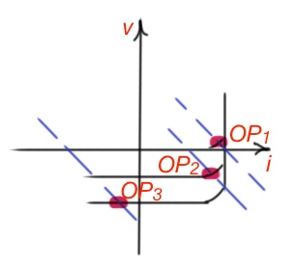
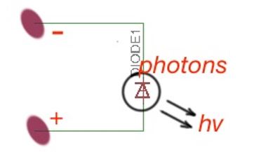
The scheme of the photodiode is depicted below. Operation point I reflects the properties of a passive device and it corresponds to the positive current and positive voltage magnitudes. Operation point II reflects the properties of a solar cell – the current for the operating point is negative, and the voltage is positive, and the diode is dissipating negative energy. The solar cell (photodiode) is a device that transforms light energy to the electrical energy. For operation, point III corresponds the photodiode regime as a lighting sensor, which means that the reverse-biased diode current flowing through it is determined by the light intensity.
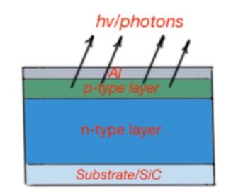
Photodiodes, used in the forward-biased regime are called light emitting diodes (LEDs). A light emitting diode has a special structure and it has its own features, that differentiate from the range of other semiconductor diodes. p- and n- layers have special metal contacts. The p-layer of an LED is slightly covered with a transparent layer to radiate light.
Unfortunately not all the photons generated in the p-n junction leave the LED heterostructure. Some part of the photons reflect from the p-layer surface inside the heterostructure, colliding with the electrons, moving them from valence to conductance band, generating the electron. The p-layer of the heterostructure is manufactured very thinly to avoid photon absorption by the semiconductor. Also it is doped in a way to contribute all the recombination processes that happen near the surface.