After the introduction of the SMU ADALM1000 let’s continue with the sixth part of our series with some small, basic measurements.
By Doug Mercer and Antoniu Miclaus, Analog Devices
Now let’s get started with the next experiment.
Objective:
The objective of this lab activity is to understand what is meant by the phase relationship between signals and to see how well theory agrees with practice.
Background:
We will investigate the concept of phase by looking at sine waves and passive components that will allow us to observe phase shift with real signals. First we will look at a sine wave and the phase term in the argument. You should be familiar with the equation: , sets the frequency of the sine wave as progresses and defines an offset in time that defines a phase shift in the function.
The sine function results in a value from +1 to –1. First set t equal to a constant—say, 1. The argument, ωt, is now no longer a function of time. With in radians, the sin of is approximately 0.7071. radians equals 360°, so radians correspond to 45°. In degrees, the sine of 45° is also 0.7071.
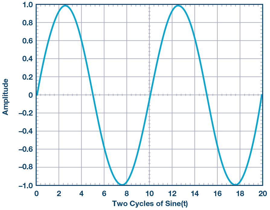
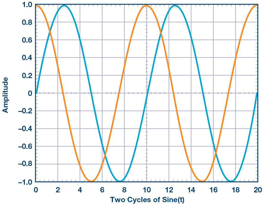
Now let t vary with time like it normally does. When the value of the ωt changes linearly with time, it yields a sine wave function as shown in Figure 1. As ωt goes from to , the sine wave goes from 0 up to 1 down to –1 and back to 0. This is one cycle or one period, , of the sine wave. The x-axis is the time varying argument/angle, , which varies from 0 to 2π.
The value of is 0 in the function plotted in Figure 2. Since the , the plot starts at 0. This is a simple sine wave with no offset in time, which means no phase offset. Note that if we are using degrees, goes from 0 to 2π or 0 to 360° to yield the sine wave shown in Figure 2.
What happens when we plot a second sine wave function in Figure 2 with , where the same value and is also 0? We have another sine wave that lands on top of the first sine wave. Since is 0, there is no phase difference between the sine waves and they look the same in time.
Now change to radians, or 90°, for the second waveform. We see the original sine wave and a sine wave shifted to the left in time. Figure 3 shows the original sine wave (green) and the second sine wave (orange) with an offset in time. Since the offset is a constant, we see the original sine wave shifted in time by the value θ, which in this example is of the wave period.
is the time offset or phase portion of Equation 1. The phase angle defines the offset in time and vice versa. Equation 2 shows the relationship. We happened to choose a particularly common offset of 90°. The phase offset between a sine and cosine wave is 90°.
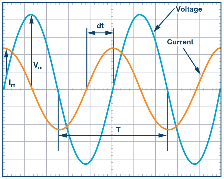
When there are two sine waves displayed, for example, on a scope, the phase angle can be calculated by measuring the time between the two waveforms (negative to positive zero crossings, or rising edges, can be used as time measurement reference points in the waveform). One full period of the sine wave in time is the same as 360°. Taking the ratio of the time between the two waveforms, dt, and the time in one period of a full sine wave, , you can determine the angle between them. Equation 2 shows the exact relationship.
Phase: .
Where T is the period of the sinusoid.
Naturally Occurring Time Offsets in Sine Waves
Some passive components yield a time offset between the voltage across them and the current through them. The voltage across and the current through a resistor are a simple time independent relationship, V/I = R, where R is real and in Ω. Thus, the voltage across and current through a resistor are always in phase.
For capacitors and inductors, the equation relating V to I is similar. V/I = Z, where Z is an impedance with real and imaginary components. We are only looking at capacitors in this exercise.
The basic rule for capacitors is that the voltage across the capacitor will not change unless there is a current flowing into the capacitor. The rate of change of the voltage (dv/dt) depends on the magnitude of the current. For an ideal capacitor, the current i(t) is related to the voltage by the following formula:
The impedance of a capacitor is a function of frequency. The impedance goes down with frequency, while, conversely, the lower the frequency, the higher the impedance.
is defined as the angular velocity: .
One subtle part of Equation 4 is the imaginary operator j. For example, when we looked at a resistor, there was no imaginary operator in the equation for the impedance. The sinusoidal current through a resistor and the voltage across a resistor have no time offset between them because the relationship is completely real. The only difference is the amplitude. The voltage is sinusoidal and is in phase with the current sinusoid.
This is not the case with a capacitor. When we look at the waveform of a sinusoidal voltage across a capacitor it will be time shifted compared to the current through the capacitor. Imaginary operator j is responsible for this. Looking at Figure 4, we can see that the current waveform is at a peak (maximum) when the slope of the voltage waveform (time rate of change ) is at its highest.
The time difference can be expressed as a phase angle between the two waveforms, as defined in Equation 2.
Note that the impedance of a capacitor is wholly imaginary. Resistors have real impedances, so circuits that contain both resistors and capacitors will have complex impedances.
To calculate the theoretical phase angle between voltage and current in an RC circuit:
where is the total circuit impedance. Rearrange the equation until it looks like:. Where and are real numbers. The phase relationship of the current relative to the voltage is then:.
Materials:
- ADALM1000 hardware module
- Two 470 Ω resistors
- One 1 μF capacitor
Procedure:
1. Set up a quick measurement using ALICE Desktop:
- Be sure the ALM1000 is plugged into a USB port and start up the ALICE Desktop
- The main screen should look like a scope display with adjustable range, position, and measurement
- Check along the bottom of the screen to be sure that CA V/Div and CB V/Div are both set to 5.
- Check that CA V Pos and CB V Pos are set to 2.5.
- CA I mA/Div should be set to 2.0 and CA I Pos should be set to 5.0.
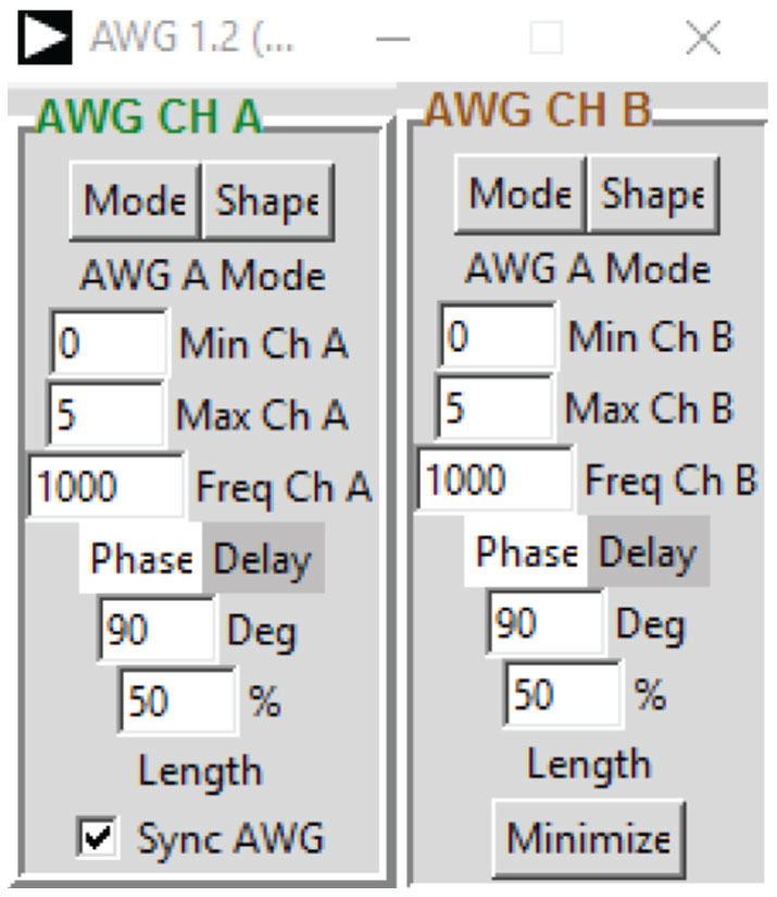
- In the AWG controls window, set the Frequency of CHA and CHB to 1000 Hz with 90° phase, 0 V minimum, and 5 V maximum values (5.000 V peak-to-peak output). Select SVMI mode and the sine waveform.
- Under the Meas drop-down, select P-P for both CA-V, CA-I, and CB-V.
- Set the Time/Div to 0.5 ms and under the Curves drop-down, select CA-V, CA-I, and CB-V.
- On your solderless breadboard, connect the CHA output to one end of a 470 Ω
- Connect the other end of the resistor to GND.
- Click on the scope Start
If the board has been calibrated correctly you should see one sine wave on top of the other, with CHA and CHB both equal to 5.00 V p-p. If the calibration isn’t correct, you might see two sine waves in phase with the amplitude of CHA different from CHB. Recalibrate if there is a significant voltage difference.
2. Measure the phase angle between two generated waveforms:
- Be sure that CA V/Div and CB V/Div are both still set to 0.5 and that CA V Pos and CB V Pos are set to 2.5.
- CA I mA/Div should be set to 2.0 and CA I Pos should be set to 5.0
- Set the Frequency of CHA and CHB to 1000 Hz with 90° phase, 0 V minimum, and 5 V maximum values (5.0 V peak-to-peak output). Select SVMI mode and the sine waveform
- In the AWG control window, change the phase, θ, of CHB to 135° (90 + 45).
- The CHB signal should look like it is leading (happening before) the CHA signal. The CHB signal crosses the 5 V axis from below to above the CHA signal. It turns out a positive θ, which is called a phase lead. The low to high crossing time reference point is arbitrary. The high to low crossing could also be used.
- Change the phase offset of CHB to 45° (90 – 45). Now it looks like the CHB signal lags the CHA
- Set the Meas display for CA to Frequency and A-B Phase. For the CB display, set it to B–A Delay.
- Set the Time/Div to 0.2 ms.
- Press the red Stop button to pause the Using the left mouse button, we can add marker point on the display.
Measure the time difference (dt) between the CHA and CHB signal zero crossings by using the markers.
- The measured dt and Equation 2 is used to calculate phase offset θ (°).
Note that you cannot measure the frequency of a signal that does not have at least one full period displayed on the screen. Usually you need more than two cycles to receive consistent results. You are generating the frequency so you already know what it is. You don’t need to measure it in this part of the lab.
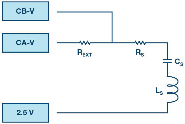
3. Measure magnitude using a real rail-to-rail circuit.
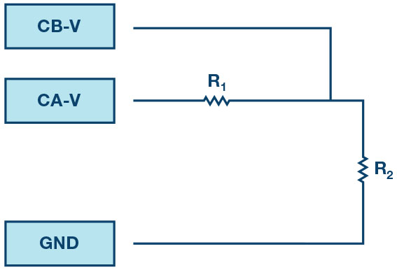
- Build the circuit shown in Figure 5 on your solderless breadboard using two 470 Ω
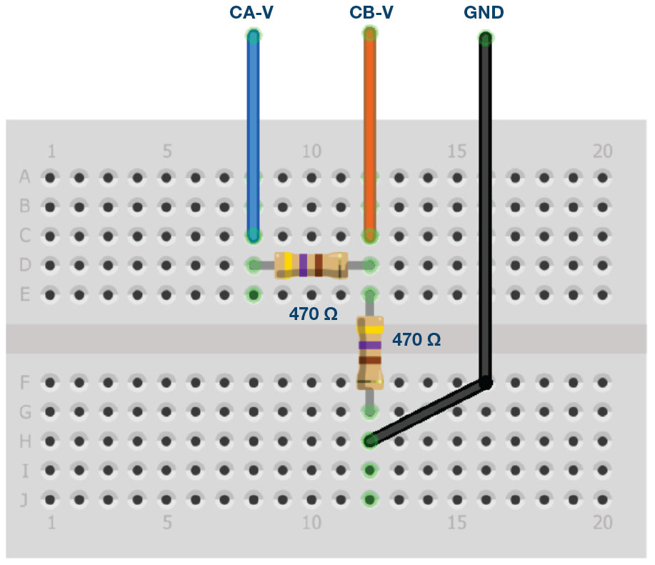
- In the AWG controls window, set the Frequency of CHA to 200 Hz with 90° phase, 0 V minimum, and 5 V maximum values (5.0 V peak-to-peak output). Select SVMI mode and the sine waveform
- Select Hi-Z mode for The rest of the settings for CHB do not matter because it is now being used as an input.
- Connect the CHA output to the CHB input and GND with the wires as shown by the colored test
- Set the Horizontal Time Scale to 0 ms/div to display two cycles of the waveform.
- Click on the scope Start button if it is not already running.
The voltage waveform displayed in CHA is the voltage across both resistors (VR1 + VR2). The voltage waveform displayed in CHB is the voltage across just R2 (VR2). To display the voltage across R1, we use the Math waveform display options. Under the Math drop-down menu, select the CAV-CBV equation. You should now see a third waveform for the voltage across R1 (VR1). To see both traces, you can adjust the vertical position of a channel to separate them. Make sure to set the vertical position back to realign the signals.
- Record peak-to-peak values VR1, VR2, and VR1 + VR2.
Can you see any difference between the zero crossings of VR1 and VR2? Can you even see two distinct sine waves? Probably not. There should be no observable time offset and, thus, no phase shift.
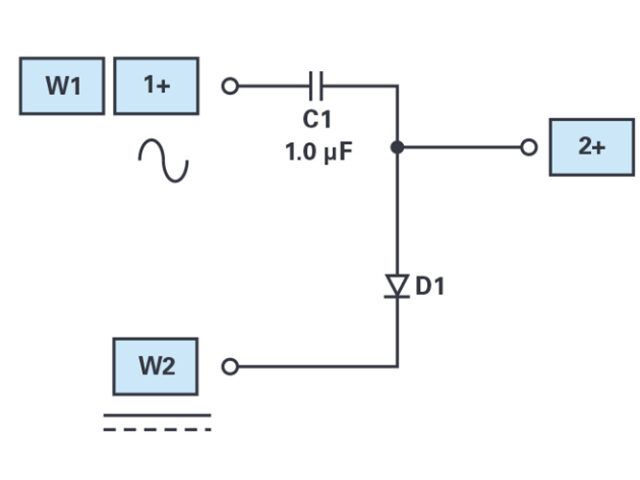
4. Measure the magnitude and phase of a real RC circuit.
- Replace R2 with a 1 μF capacitor C1.
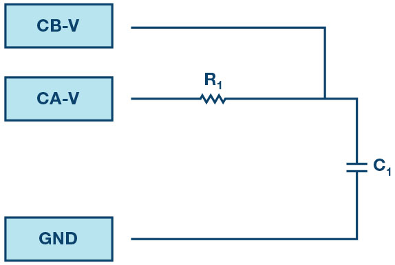

- In the AWG controls window, set the Frequency of CHA to 500 Hz with 90° phase, 0 V minimum, and 5 V maximum values (5.0 V peak-to-peak output). Select SVMI mode and the Sin waveform
- Select Hi-Z mode for CHB.
- Set the Horizontal Time Scale to 5 ms/div to display two cycles of the waveform.
Because there is no direct current through the capacitor, we have to handle the average (dc) values of the waveforms differently.
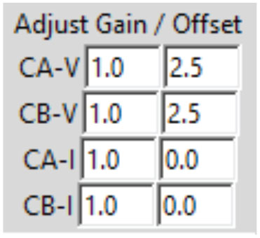
- On the right-hand side of the main screen there are places to enter a dc offset for Channel A and Channel Set the offset values as shown in Figure 9.
- Now that we have removed the offset from the inputs, we need to change the vertical position of the waveforms to recenter them on the grid. Set CA V Pos and CB V Pos to 0.
- Click on the scope Start button if it is not already running.
- Measure CA-V, CA-I, CB-V, and math (CAV – CBV) peak-to-peak. What signal is the math waveform?
- Record VR1, VC1, IR1, and VR1 + VC1.
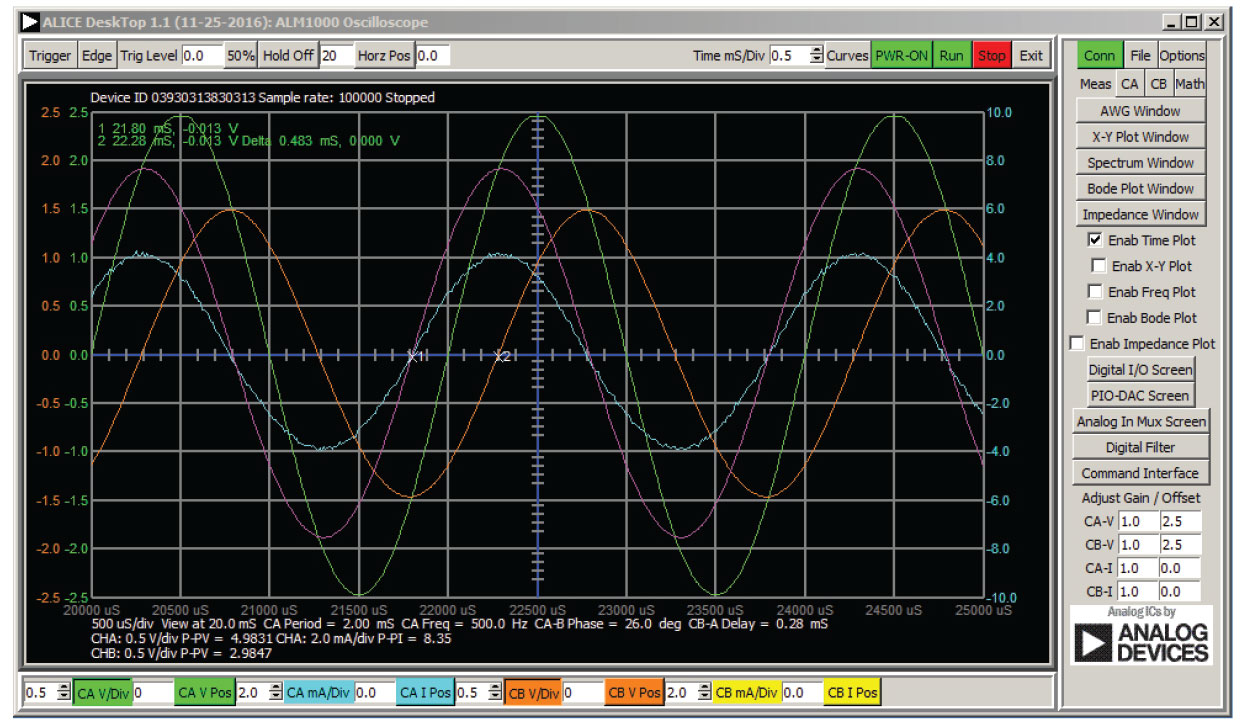
Now let’s move on to doing something with phase. Hopefully you see a few sine waves with time offsets or phase differences displayed on the grid. Let’s measure the time offsets and calculate the phase differences.
- Measure the time difference between VR1, IR1, and VC1 and calculate the phase
- Use Equation 2 and the measured dt to calculate the phase angle θ.
The markers are useful for determining dt. Here’s how.
- Display at least 2 cycles of the sine waves.
- Set the Horizontal Time/Div to 0.5 μs. Be sure to click on the red Stop button before trying to place markers on the grid.
Note that the Marker Delta display keeps track of the sign of the difference.
You can use the measurement display to see the frequency. Since you set the frequency of the source, you don’t need to depend on the measurement window for this value.
Assume dt is 0 if you can’t see any difference with one or two cycles of the sine wave onscreen.
- Put a first marker at the negative to positive zero crossing location for the CA-V (VR1 + VC1) Put a second marker at the nearest negative to positive zero crossing location for the math (VR1) signal. Record the time difference (dt) and calculate the phase angle (θ). Note that dt may be a negative number. Does this mean the phase angle leads or lags?
To remove the markers for the next measurement, click on the red Stop button.
- Put a first marker at the negative to positive zero crossing location for the CA-V (VR1 + VC1) Put a second marker at the nearest negative to positive zero crossing location for the CB-V (VC1) signal. Record the time difference (dt) and calculate the phase angle (θ).
- Put a first marker at the negative to positive zero crossing location for the math (VR1) Put a second marker at the nearest negative to positive zero crossing location for the CB-V (VC1) signal. Record the time difference (dt) and calculate the phase angle (θ).
Is there any measurable time difference (phase shift) between the math (VR1) signal and the displayed CA-I current waveform? Since this is a series circuit, the current sourced by AWG Channel A is equal to the current in R1, and C1.
Questions:
- Using Equation 5 and Equation 6, determine the impedance (Zcircuit) and phase (θ) relationship of the current relative to the voltage for a RC circuit by replacing the A and B variables with proper values.
- For the RC circuit in Figure 7, measure the time difference and calculate the phase θ offset at 1000 Hz frequency.
You can find the answers at the StudentZone blog.
Appendix:
Notes
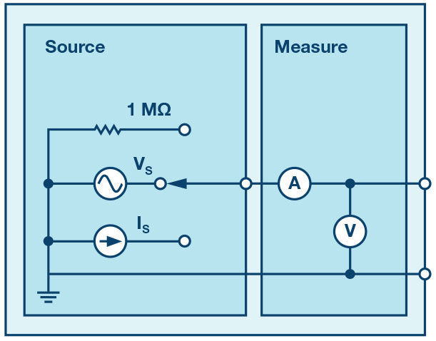
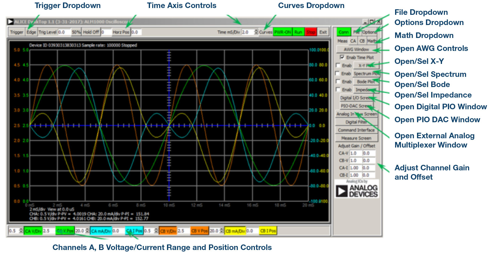
As in all the ALM labs, we use the following terminology when referring to the connections to the ALM1000 connector and configuring the hardware. The green shaded rectangles indicate connections to the ADALM1000 analog I/O connector. The analog I/O channel pins are referred to as CA and CB. When configured to force voltage/measure current, –V is added (as in CA-V) or when configured to force current/measure voltage, –I is added (as in CA-I). When a channel is configured in the high impedance mode to only measure voltage, –H is added (as in CA-H).
Scope traces are similarly referred to by channel and voltage/current, such as CA-V and CB-V for the voltage waveforms, and CA-I and CB-I for the current waveforms.
We are using the ALICE Rev 1.1 software for those examples here. File: alice-desktop-1.1-setup.zip. Please download here.
The ALICE Desktop software provides the following functions:
- A 2-channel oscilloscope for time domain display and analysis of voltage and current
- The 2-channel arbitrary waveform generator (AWG) controls.
- The X and Y display for plotting captured voltage and current voltage and current data, as well as voltage waveform histograms.
- The 2-channel spectrum analyzer for frequency domain display and analysis of voltage
- The Bode plotter and network analyzer with built-in sweep generator.
- An impedance analyzer for analyzing complex RLC networks and as an RLC meter and vector
- A dc ohmmeter measures unknown resistance with respect to known external resistor or known internal 50 Ω.
- Board self-calibration using the AD584 precision 2.5 V reference from the ADALP2000 analog parts kit.
- ALICE M1K voltmeter.
- ALICE M1K meter source.
- ALICE M1K desktop tool.
For more information, please look here.
Note: You need to have the ADALM1000 connected to your PC to use the software.
Doug Mercer [doug.mercer@analog.com] received his B.S.E.E. degree from Rensselaer Polytechnic Institute (RPI) in 1977. Since joining Analog Devices in 1977, he has contributed directly or indirectly to more than 30 data converter products, and he holds 13 patents. He was appointed to the position of ADI Fellow in 1995. In 2009, he transitioned from full-time work and has continued consulting at ADI as a Fellow Emeritus contributing to the Active Learning Program. In 2016 he was named Engineer in Residence within the ECSE department at RPI.
Antoniu Miclaus [antoniu.miclaus@analog.com] is a system applications engineer at Analog Devices, where he works on ADI academic programs, as well as embedded software for Circuits from the Lab® and QA process management. He started working at Analog Devices in February 2017 in Cluj-Napoca, Romania. He is currently an M.Sc. student in the software engineering master’s program at Babes-Bolyai University and he has a B.Eng. in electronics and telecommunications from Technical University of Cluj-Napoca.