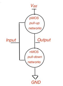
This post answers the question “What is CMOS gate logic?”. A CMOS gate is a system consisting of a pMOS pull-up network connected to the output 1 (or VDD) and nMOS pull-down network, connected to the output 0 (or GND). Schematically a CMOS gate is depicted below. Previously we discussed the simplest forms of CMOS gates – inverter and NAND gates.
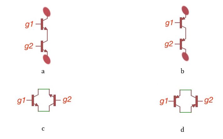
From here we know that if all of the seriously connected transistors are ON, all the network of these transistors are ON. If at least one of the parallel connected transistors is ON, all the parallel network is ON. Combining these constructions we can get some complex structures. When connecting pull-up and pull-down network, they both try to make an output.
The possible results are shown in Table 1. Here, high impedance (or Z floating) is possible as an output if pull-up and pull-down networks are both OFF. If the pull-up and pull-down networks are both ON, we are getting the crow-barred X result. The connection between pull-up and pull-up networks results with output and power dissipation, as it is a physical process. Figure 2 shows the results of all the possibilities for the connection of series and parallel transistors.
Table 1.
| Pull-down OFF | Pull-down ON | |
| Pull-up OFF | High Impedance (Z floating) | 0 |
| Pull-up ON | 1 | Crowbarred X |
The n-input NOR gate: has a truth table (Table 2) and schematically is depicted in Figure 3. In terms of operation, if any input is high, the result is low, if all the inputs are low – the result is high.
Table 2.
| A | B | … | X | Y |
| 0 | 0 | 0 | 0 | 1 |
| 0 | … | … | 1 | 0 |
| 0 | 0 | 1 | 1 | 0 |
| 0 | 1 | 1 | 1 | 0 |
| 1 | 1 | 1 | 1 | 0 |
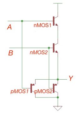
A Compound gate is a structure experiencing more complex logic functions in a single state and formed by combinations of transistors connected in series and parallel. Another important term is the conduction complements, which is the interchanging operations. When transistors appear parallel in the pull-down network, they appear in series in the pull-up network and reverse.
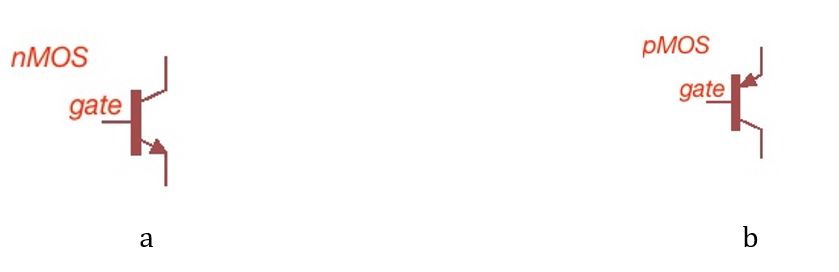
Other important parameters are Pass transistors and Transmission gates. In our logical schemes, the sources VDD and GND are the strong sources 1 and 0. An nMOS transistor is strong 0, and weak 1 (it can also be called degraded).
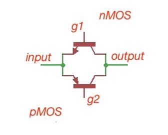
And the pMOS transistor is strong 1 and weak 0. A Pass transistor exists when an nMOS or pMOS transistor is used alone with an imperfect switch. When nMOS and pMOS transistors are combined in parallel, it is called a Transmission gate or Pass gate. In this case the switch is on when the gate is 1.
Figure 4 shows a pass transistor with strong and weak outputs. And Figure 5 shows a Transmission gate input and output. Another important term is Fully restored logic, which is when a nMOS transistor only carries 0, the pMOS transistor only carries 1, and the output is strongly driven and never degrades.
Static CMOS gates are very useful in logic design. They do not dissipate power in contrast to other different technologies. And the idea of a CMOS gates, as mentioned above, is to invert the signal. This inversion occurs without power dissipation which makes the technology very useful. Different operations can be built using CMOS gates in multiple stages. CMOS gates can also perform non-inverting functions when combined properly.
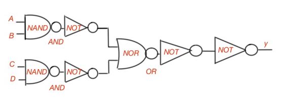
Compound gates are always better to use in logic designs instead of a variety of AND/OR and other gates. Figure 6 depicts the logic function AOI22 with two variations – with AND/OR/NAND gates and compound gates. The last one makes design easier.
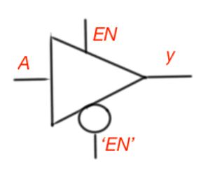
The Figure below depicts the symbol for a tristate buffer. This structure works in the following way: when input EN is 1, then output Y is equal to the input A. When EN is 0, Y is floating Z. In some cases the tristate buffer also has a complimentary EN input. The truth table for a tristate buffer shown in Table 3.
Table 3.
| A | Y | |
| 1/0 | 0 | 0 |
| 1/0 | 1 | 1 |
| 0/1 | 0 | Z |
| 0/1 | 1 | Z |
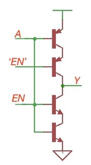
Figure 7 also depicts the structure. The transmission gate is built with two transistors with the same truth table like the tristate buffer. This transmission gate is a non–restoring system, and it has power losses, in contrary to the tristate buffer. Another important structure is a tristate inverter (Figure 8). The output is driven by the VDD or GND. This is a restoring system, which means it is power lossless. Tristates are a great asset for multiple logical unit designs, especially when it is needed to drive the same bus.
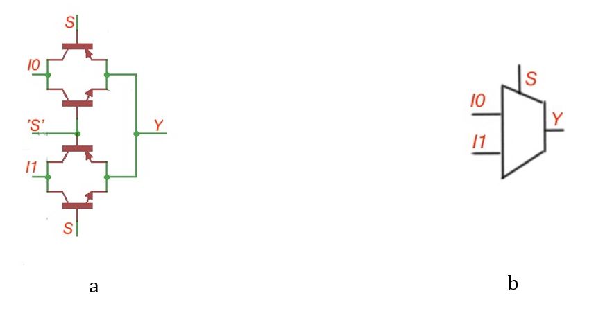
Multiplexer is a CMOS memory component. It chooses the output from several values on a select signal. The truth table for a 2-input multiplexer is shown in Table 4.
Table 4. The 2-input multiplexer truth table:
| 1/0 | 1 | X | 1 |
| 1/0 | 0 | X | 0 |
| 0/1 | X | 1 | 1 |
| 0/1 | X | 0 | 0 |
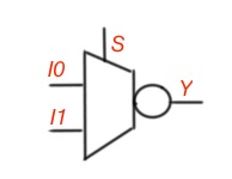
The scheme and principle of the operation of a multiplexer is shown in Figure 9. The inverting multiplexer can be presented with several ways – using a compound gate, the tristate inverter or the inverting multiplexer itself.
More educational content can be also accessed via Reddit community r/ElectronicsEasy.