This post tells about types of delay in VLSI. When designing semiconductor devices it is very important to take into consideration the speed and power.
When designing the delays in VLSI it is important to take into consideration the following parameters:
- Propagation delay time
- Contamination delay time
- Rise time
- Fall time
- Edge rate
Regarding gates, charging and discharging a node is called the driver, the gate’s wire driven is the load. The propagation delay is called the delay.
The timing analyser computes the signal arrival time. The nodes are classified as the inputs, outputs and internal nodes. The signal arrival time should be taken into consideration and the time data is required at the outputs. The arrival time at the internal node depends on the propagation delay at the gate and the arrival times of the inputs at the gates.
The timing analyser calculates the arrival times at each internal node and checks if the outputs arrive at their required times. The difference between the required and arrival time is the slack. A negative slack means that the circuit meets the required timing. Arrival times can also be calculated based on the contamination times. The summarised data gives the picture of the gate switching parameters.
Timing optimisations.
The design structures must always contain the paths that are fast enough or the ones that are critical in terms of the operating times – they are called critical paths. The critical paths can be affected at the following levels:
- Architectural level;
- Logic level
- Circuit level
- Layout level.
The best leverage is performed with the good microarchitecture. This level requires the broad knowledge of the both the algorithmic and technological level of the device. The next level is logic. The trade-offs can be made at the stage of the functional blocks, the number of stages of gates in the clock cycle, and at the fan-in and fan-out cycles. The delay can be also be turned at the circuit level, varying the transistor size or using different CMOS techniques. The last level is layout level, when the delay can be set up. Here the delay can be set up with the wiring lengths.
Many device designers never leave the RTL level that creates the design. The standard way to write RTL code is to synthesise it and check if the results are fast enough. The timing analysers are used to check the timing closure, and whether the circuit meets the timing requirements. The lower abstraction level is the best way to adjust and vary the timing parameters.
Transient response
How to calculate delay in two steps:
- to develop the physical model of the circuit,
- write the differential equation for the circuit voltage and time.
The solution of this differential equation is called transient response. And the delay is the time when the output voltage reaches .
The differential equation is based on the charged and discharged capacitance of the circuit. The capacitance current is . Every real circuit has a capacitance that has to be taken into consideration – these are defined as gate capacitance and diffusion capacitance.
A very useful model of estimating the capacitance in a circuit is the RC delay model in VLSI. This model approximates the non–linear transistor I-V and C-V characteristics, taking into account the average resistance and capacitance over the switching time of the gate. The RC delay model considers the transistor as the switch with the resistor in series. The effective resistance is equal to the ratio during the switching process.
RC delay model in VLSI
The RC delay model is a metric used in VLSI design to calculate the signal delay between the input voltage and output voltage of the input signal. The input signal is a step function. In this case the transistor can be considered as a switch in series with a resistor.
A unit nMOS transistor is characterised with resistance or effective resistance . Let’s consider a k times transistor unit, here the resistor of the single transistor is , is the constant here. pMOS transistor has a bigger resistance – .
nMOS transistors are characterised with higher mobility than pMOS transistors. If the transistor is velocity-saturated, its current and resistance does not depend on the channel length.
Let’s consider a transistor with gate capacitance C. For a k unit cell, gate capacitance of the transistor is kC. Diffusion capacitance usually depends on the size of drain/source, but with the most common approximation it is also C.
Figure 1 shows the equivalent RC circuits for nMOS and pMOS transistors. Figure 2 shows a fanout-1 inverter and its equivalent circuit.
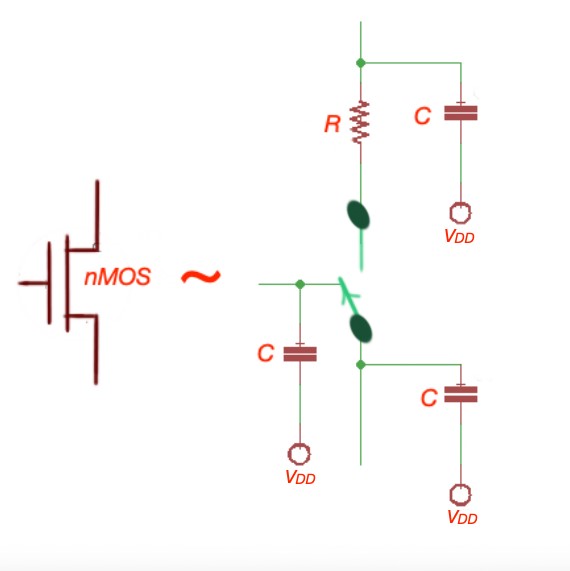
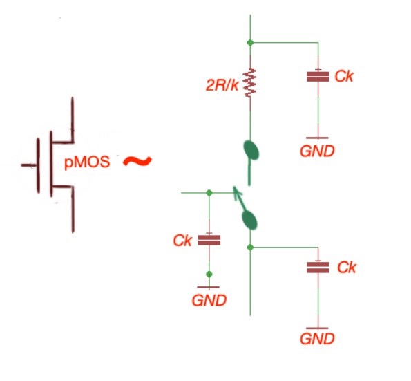 Figure 1. nMOS and pMOS transistors and their RC equivalent circuits.
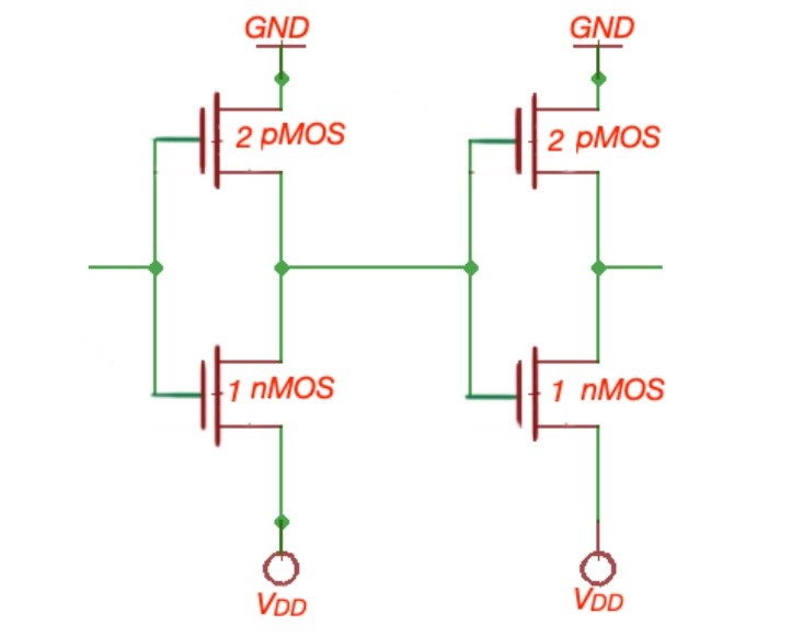
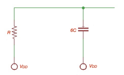
Figure 2. Inverter gate and its equivalent representation.
Educational content can also be reached via Reddit community r/ElectronicsEasy.