This post is about how memory spaces are constructed. Embedded processors are characterised with hierarchical memory architectures, combining different sizes and performance memory.
Memory of the processor is L1 memory and operates on the core-clock rate. L1 memory can be divided into data and instruction memory. Here data memory runs at core-clock rate, and supports single-cycle access, and instruction memory supports instruction evaluation of a single cycle.
L1 memory usually limited in size, and supported with on- or off-chip memory with increased latency.
Larger on-chip memory is called L2 memory.
External memory is called L3 memory.
Speed correlation between L1, L2 and L3 types of memory are depicted below. L1 can comprise 10s of kbytes, L2 – 100s of kbytes, L3 – 100s of Mbytes.
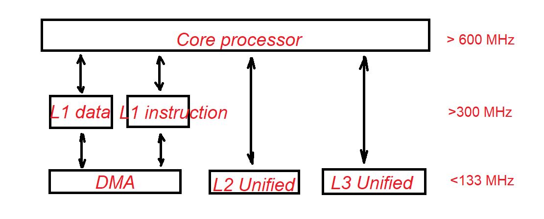
How L1, L2, L3 memory spaces are constructed.
L2 and L3 are unified memories, so data and instruction can be accessed from the common memory space.
L1 and L2 memories are running at CCLK rate and L3 runs at SCLK rate.
You can also access our educational content from the Reddit community r/ElectronicsEasy.