Synchronous DRAM memory is the highest performance external memory, that allows to store large amounts of data without losing performance. SDRAM also stands for SDR SDRAM (Single Data Rate SDRAM).
SDRAM is a synchronous DRAM memory, it is synchronised with clock speed of the processor. It is consist of banks, rows, and columns.
The SDRAM block diagram is depicted below.
Modern SDRAM runs at 3.3V, having clock rates from 133MHz up to 200 MHz. SDRAM bus width can be x8, x16, x32. SDRAM density has direct correlation with bus width, every SDRAM is characterised with a depth, where for example, 128Mb SDRAM has 16Mb depth and x8 bus width.
SDRAM consist of rows and columns at the lowest level. First row should be opened, it becomes active then column can be selected, and data can be transferred.
SDRAM consist of 4 internal banks.
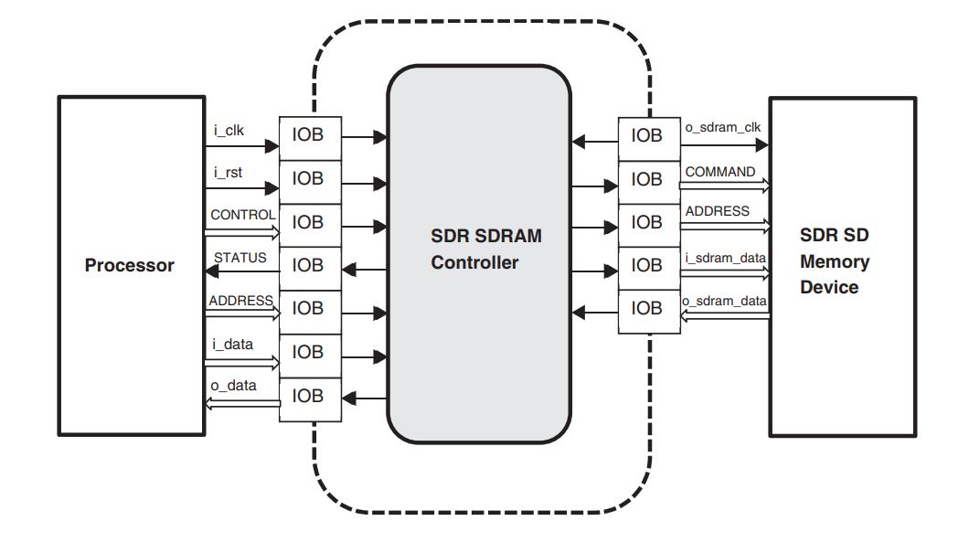
SDRAM controller uses external pins to issue series of commands to SDRAM. SDRAM pins are:
- ADDR
- DATA
- SDQM
- SA10
- SCKE
- CLKOUT
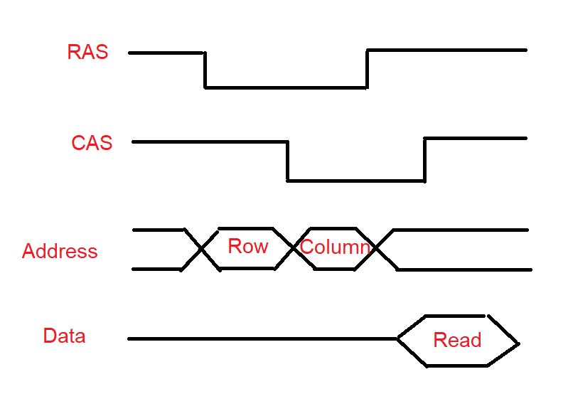
The diagram below describes SDRAM transaction.
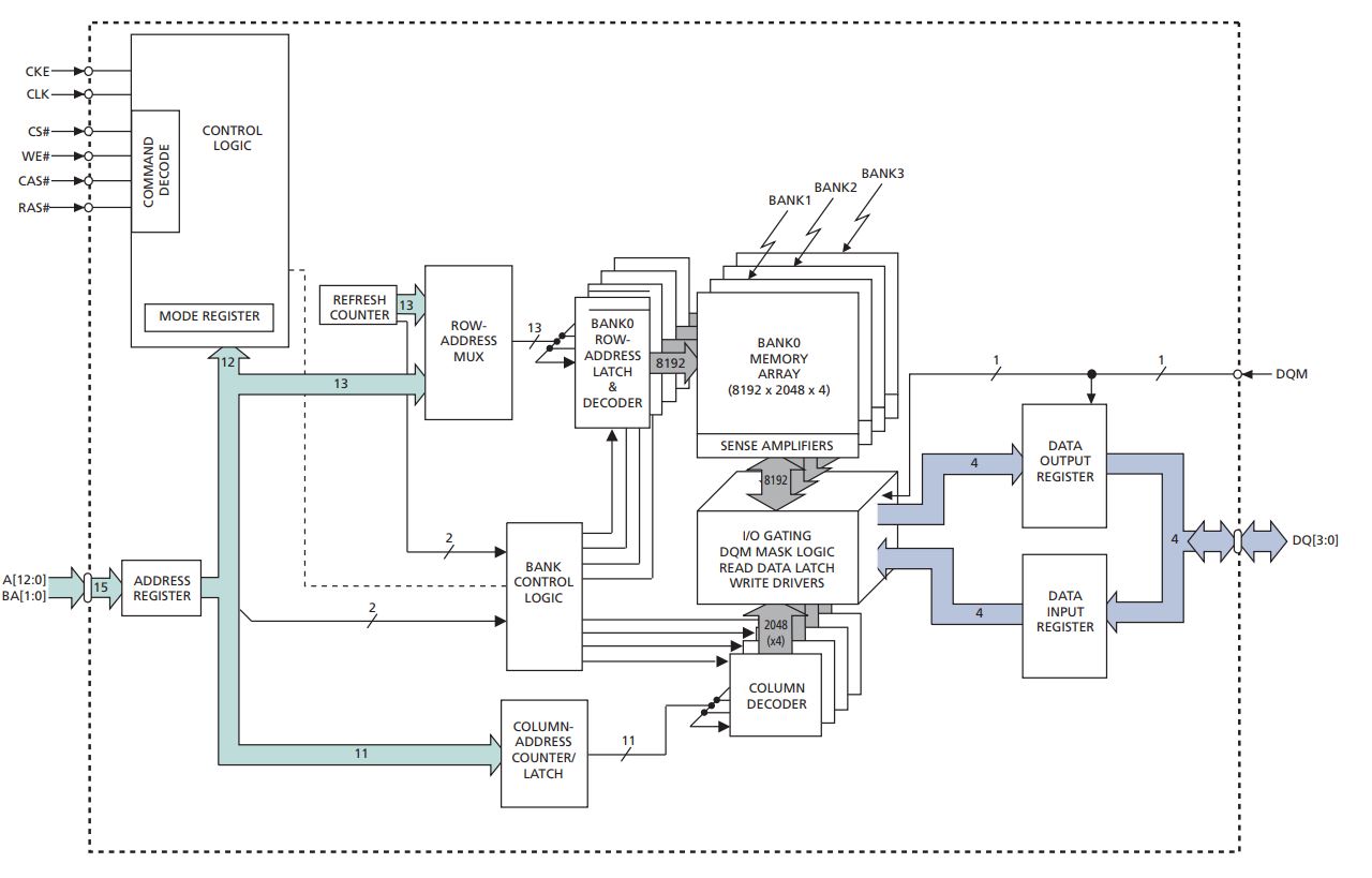
The system block diagram for SDR SDRAM controller is depicted below.
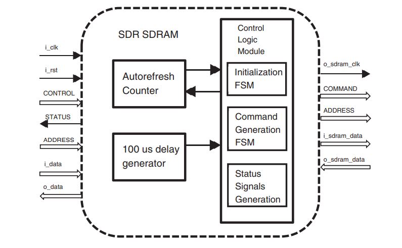
Functional block diagram of the SDR DRAM is depicted below.
Before performing commands the SDR SDRAM should be initialized, that demands a set of certain steps[1] :
- Idle state;
- waiting time;
- Precharge all the the banks;
- Precharge period () waiting time;
- Auto Refresh command starts;
- Auto Refresh period () waiting time;
- Second Auto Refresh command;
- Auto Refresh period () waiting time;
- Load Mode Register;
- Load Mode Register delay
- Finish of initialization.
After these steps General commands can be performed.
Here are several commands SDRAM controller uses communicating with memory device:
Bank Activate – command that has to be activated before applying Write and Read commands. It makes SDRAM to open certain internal bank.
Precharge – command closes specific internal bank.
Precharge All – command closes all internal banks.
Read/Write – commands initiating read/write access in the active page. There is a delay between Bank Activate and Read/Write commands, that is determined by .
Load Mode is a command used to initialise SDRAM chip.
Auto-Refresh command determine the way the contents of SDRAM refreshed periodically.
Self-Refresh is a command that determine the way contents of SDRAM refreshed periodically.
When choosing SDRAM very important parameter to pay attention to is CAS (Column Address Strobe) Latency, that can also be named as CL2 and CL3, that is a delay in clock cycles between moment when SDRAM detects Read command and when it provides data. CAS Latency should be large than (column access time).
SDRAM controller has a refresh counter, that is responsible for refresh command of the SDRAM. Here Precharge All banks command starts, and then Auto-Refresh command goes.
Our educational content can be also accessed via Reddit community r/ElectronicsEasy.
[1] SDR SDRAM Controller Lattice Semiconductor, RD1174