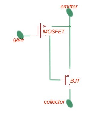
This post answers the question what is the power IGBT. IGBT is the combination of two discrete devices – MOSFET and BJT.
This approach to the semiconductor technology gives excellent output characteristics, great SOA and very good switching time, compared to discrete devices themselves. The power IGBT structure is depicted in Figure 1.
Figure 1. The electrical equivalent scheme of the IGBT.
A simplified structure of the device can be seen in Figure 1b. This vertical structure of the device offers the possibility to obtain the greater current densities and lower forward voltage drop. The , and are combined in the BJT device. This device has low current gain. The operation of the power IGBT can be easily seen if we will operate the BJT with the voltage of the gate.
2. If the gate is shortened to the emitter the device is OFF.
3. If the gate is positive, and bigger than the , then the device is ON.
In addition, et’s look at the layer structure of the IGBT (Figure 2), the static characteristics of the drift region is expressed with the formula: , this depends on the charge carriers in the power IGBT, and other static characteristics.
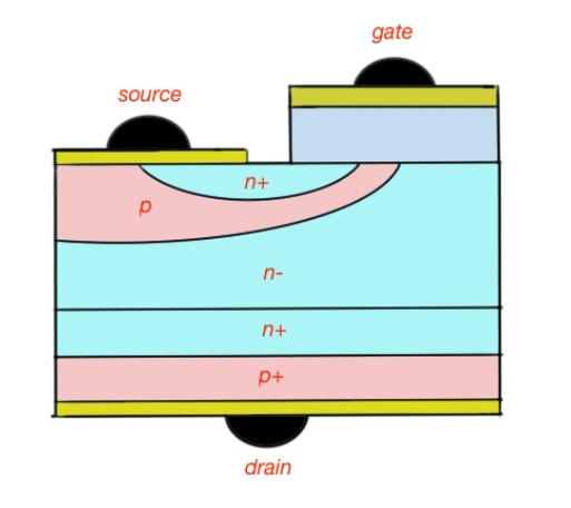
a – layer scheme of power IGBT
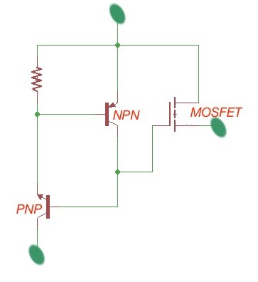
b – equivalent scheme of power IGBT
The power IGBT can be present with the following equivalent circuits, depicted in Figure 2.
Power IGBT characteristics
These characteristics are usually provided in the manufacturer’s datasheet, are:
- Collector-emitter blocking voltage ;
- Emitter-collector blocking voltage ;
- Gate-Emitter voltage ;
- Continuous collector current ;
- Peak collector repetitive current ;
- Maximum power dissipation ;
- Junction temperature ;
- Clumped collective inductor current ;
- Collector-emitter leakage current ;
- Gate-emitter threshold voltage ;
- Collector-emitter threshold voltage ;
- Forward transconductance ;
- Total gate charge ;
- Turn-on delay time ;
- Rise time ;
- Turn-off delay time ;
- Input and output capacitances and ;
- Reverse transfer capacitance ;
- Safe-operation area SOA.

