This posts tells about static induction transistor construction. Invented by J. Nishizawa in 1975, the static induction devices were first successfully fabricated in Japan. Among the static induction devices, a static induction transistor (SIT) is regarded as a JFET device conducting in the pre-punch-through region.
Static Induction Devices (SID) are a static induction family that includes static induction transistor (SIT), static induction thyristor, static induction diode (SID), static induction transistor logic (SITL), space charge limiting load (SCLL), and static induction MOS transistor (SIMOS). The static induction devices are current-controlled devices by both potential barrier and space charge.
Static induction transistors are characterised with the following features:
- Feature outstanding operating qualities
- Have frequencies up to 1THz
- Belong to great switching speed
- Low switching energy
- Large reverse voltage
- Low forward voltage drop features
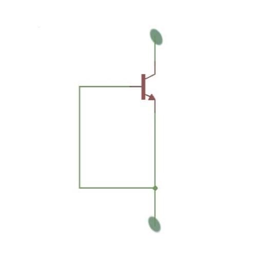
SIT is shown schematically on figure 1. The working process of a SIT is that SIT electrostatically instigates a potential interruption in the device as well as maintains the electricity between the drain and source.
In a SIT, where the mall electrostatic field prevails in the region of the potential interruption, the current flow and diffusion through the device can be explained with the following formula , here is the carrier concentration for .
The potential can be explained comparatively with the function of the second-order along with the static induction transistor channel and across the transistor channel by the formulas and
are for two-channel dimensions, where is thought as the height of the potential interruption.
The drain current through the transistor is , where is thought as the concentration of the source, and are thought as the geometrical properties of the potential saddle of the interruption. Here is always considered as a function of the gate and drain voltages.
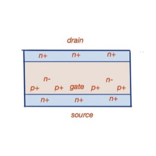
SIT features a low forward voltage drop and can be created by lessening the emitter to the gate of the SIT that’s exposed on the figure below.