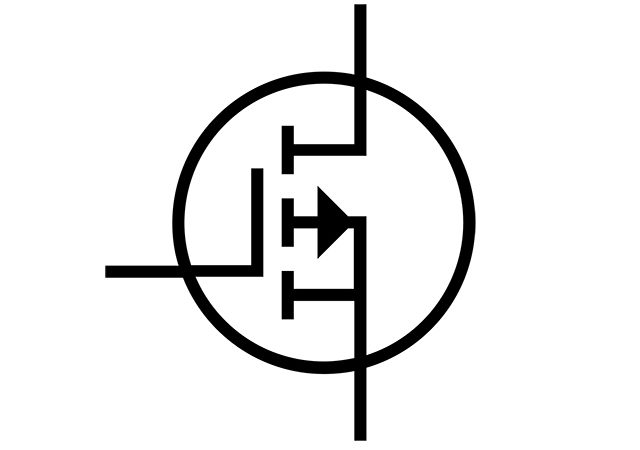
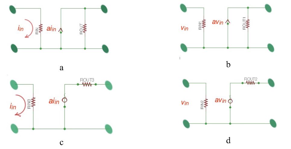
A transistor is a three-terminal semiconductor device that can perform amplification and switching functions. The operation of a transistor as a linear amplifier is schematically described below. There is four possible modes of transistor operation as a linear amplifier – current-controlled current source, voltage-controlled current source, current-controlled voltage source and voltage-controlled voltage source.
The current and voltage sources exist in order to generate the current or voltage output level proportional to the input with the certain constant, which is called the gain of the transistor. The bipolar junction transistor (BJT) plays the role of the current-controlled amplifier, the field-effect transistor (FET) plays role of the voltage-controlled amplifier.
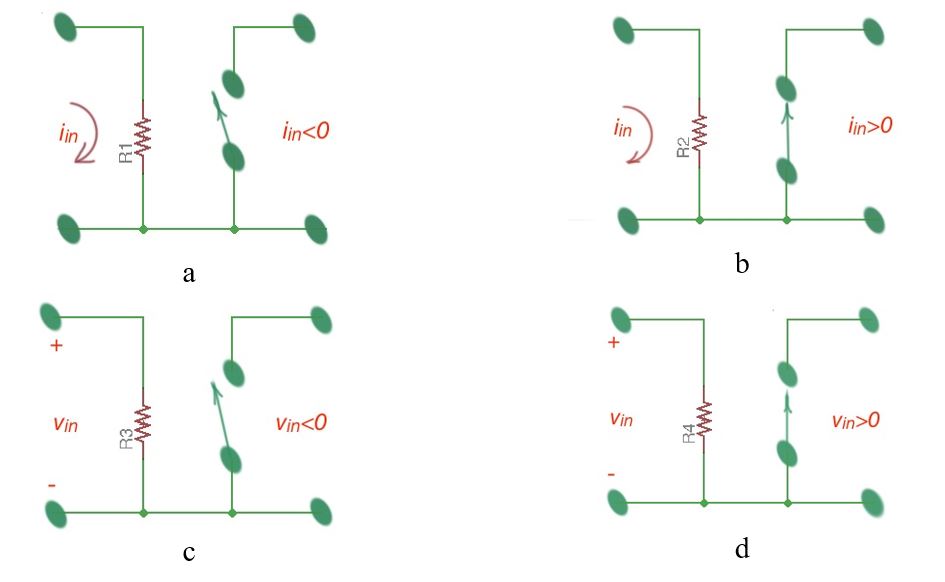
In the non-linear mode transistors act as current-controlled and voltage-controlled switches (below).
Bipolar junction transistor
The two-terminal p-n junction is the basis for a great variety of more complex semiconductor devices, and the bipolar junction transistor is one of them. The BJT is made by combined semiconductor materials with different doping levels, i.e. it can be formed by the -layer situated between p- and p+ -layers, or p-layer between n– and n+ -layer. These BJTs are called pnp and npn transistors respectively. Schematically these two transistors are depicted below.
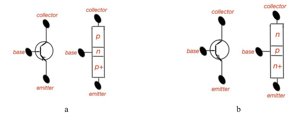
The transistor’s work may be understood easily if you recon previous section on how a pn-junction works. Let’s consider a situation where for transistor – the base-emitter junction operates like a classical junction, or diode, being forward-biased. The electrons will flow from the emitter to the base, and the holes will flow from base to an emitter.
Here the flow of electrons is heavier, because the layer is more heavily doped. The base here should be much thinner than the emitter. The electrons emitted by the emitter, passing through the base, experience a small recombination. The rest of the of electrons go to the collector and collect there.
So we have a strong current flow from the emitter to the collector oppositely directed to the electron flow. The KCL for the junction is:
As mentioned above the -transistor operates in the same way as a npn-transistor above, but the charge carriers are reversed. The precise design and operation details of transistors are presented in the VLSI design part of the course.
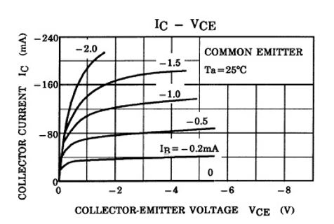
So, as the transistor is the three-terminal device, two currents and two voltages are sufficient to describe its operation. To do that we must use the KCL and KVL equations. Similarly to that, we must use two characteristics – base current – base-emitter voltage, and collector current – collector-emitter voltage. Figure 4 depicts the typical volt-ampere characteristics for the BJT Toshiba transistor 2SA1162.
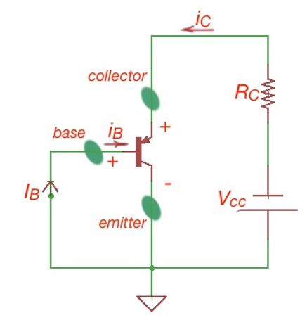
Let’s consider how to determine the operational region of the transistor in a linear mode. Figure below depicts the simple electric circuit for a transistor. Let’s assume we know the voltages . It gives us a voltage emitter-base and this voltage can tell us if the base-emitter junction is forward- or reverse-biased, and the collector-emitter voltage . Also, we can determine collector and base currents . Finally we can determine the amplification coefficient .
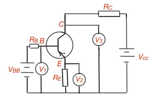
Let’s consider how to determine the operation point of a BJT transistor. Figure below depicts an ideal circuit for a DC biased transistor. It is characterised by the set of curves, where the certain value of base current corresponds to a certain i curve. The proper selection of base current and emitter current makes it possible to determine the transistor operation point . Here . So .
So here we can find the crossing of and that will lead us to the transistor’s operating point .
