A MOS-device is a simplified example of a MOSFET structure (without source and drain). Let’s consider how the MOS-device works. The simplest MOS-device has the Metal-Oxide-Silicon structure and is shown in Figure 1.
This structure is similar to a capacitor – there is an oxide layer between the metal contact and substrate, and is called a MOS-capacitor. The substrate is also equipped with a metal contact which is grounded. The substrate is a doped Si, and the isolator is a silicon dioxide.
Let’s consider the device with a p-type substrate. This device is called an nMOS. By varying the applied voltage V we can obtain several regimes of the MOS capacitor (Figure 2).
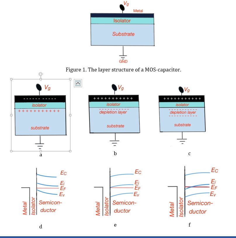
If voltage then the MOS device is in the accumulation mode. The picture of bands of the MOS structure is flat, and the Fermi level is stable – Figure 2a. When the voltage reaches the value where the energy bands are absolutely flat, this voltage is called flatband voltage VFB.
If voltage slightly increases, this is a depletion mode. Here positive charges exist on the gate side, and negative charges collect on the substrate side, creating a depletion layer. As the potential is increases, more negative charges accumulate in the substrate – Figure 2b. We can obtain the width of the depletion layer from the Poisson equation, taking into consideration that depletion mode considers the high quantity of acceptors concentration where LD is called a Debey length, and is a potential of the interface substrate-isolator.
If the voltage growth is high, and the Fermi level approaches the conduction band, Figure 2c, the inversion mode begins. In this case more electrons accumulate on the interface substrate-isolator. When the applied voltage to the gate continues to increase we finally get a strong inversion mode, when the concentration of negative charges at the interface is much higher than the dopant ions concentration Na A strong inversion mode will be reached when the substrate-isolator potential where is the Fermi potential.
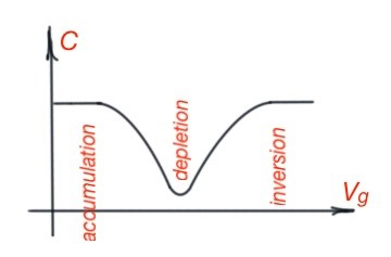
The capacitance of the considered MOS-structure is an interconnection of the insulator layer and semiconductor layer. During accumulation mode the capacitance of the MOS structure is determined by the capacitance of the isolator layer .
During depletion mode the capacitance of the MOS structure is formed by two capacitance – the isolator layer and depletion layer of the semiconductor. is a Si substrate permittivity, xdep is the depletion layer width.
Note that the total capacitance is less than the isolator layer capacitance. At the inversion layer the concentration of electrons at the interface of the isolator-substrate is so high that the substrate capacitance can be ignored. So . The capacitance dependence of the gate voltage is depicted in Figure 3.
(«MOSFET device Physics and operation», Prof. Shayla Sawyer.; «Silicon Integrated Circuits», Part A, John R. Brews).