Written by Doug Mercer, Consulting Fellow, and Antoniu Miclaus, System Applications Engineer, Analog Devices.
Objective
The objective of this lab activity is to measure the voltage-dependent capacitance of a reverse-biased PN junction.
PN junction capacitance
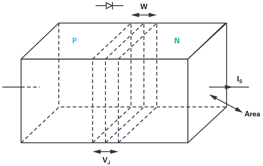
Increasing the reverse bias voltage, VJ, across a PN junction leads to the redistribution of charge away from the interface, leaving a depleted region or layer, W, in Figure 1. This depleted layer acts like the insulator between the two conducting plates of a capacitor. The thickness of this layer, W, is a function of the applied electric field and the doping concentration. The PN junction capacitance is divided into two components, the barrier capacitance, and the diffusion capacitance. Under the conditions of reverse-bias, free carrier injection does not occur; therefore, the diffusion capacitance is equal to zero. The barrier capacitance is the dominant source of capacitance for reverse and small positive-bias voltages less than the diode turn on voltage (0.6V for silicon). In practice, the barrier capacitance can be as small as a fraction of a picofarad to hundreds of picofarads depending on the area of the junction and the doping concentration. The dependence of the junction capacitance to the applied bias voltage called the capacitance-voltage (CV) characteristic of the junction. In this lab, you will measure and plot this characteristic for various PN junctions (diodes).
Figure 1. PN junction depletion region.
Materials
- ADALM2000 active learning module
- Solderless breadboard
- One 10kΩ resistor
- One 39pF capacitor
- One 1N4001 diode
- One 1N3064 diode
- One 1N914 diode
- Red, yellow, and green LEDs
- One 2N3904 NPN transistor
- One 2N3906 PNP transistor
Directions step 1
Build the test setup as shown in Figure 2 and Figure 3 on your solderless breadboard. The first step is to measure the unknown capacitance Cm with the known C1 we connected between the AWG output and scope input. The two scope minus inputs 1– and 2– are both grounded. The scope channel 1+ input is tied to the AWG1 output, W1, using one row on the breadboard. Scope channel 2+ is inserted into a breadboard row 8 to 10 rows away from the row that the AWG output is inserted in. The row adjacent to scope channel 2+ and toward the AWG1 row is grounded. This is to minimise any unwanted stray coupling between AWG1 and scope channel 2. Because the fly-wires are not shielded, try to keep the W1 and 1+ wires as far away from the 2+ wires as possible.
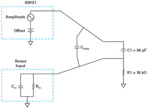
Figure 2. Step 1 setup to measure Cm.
Hardware setup
Using the network analyser instrument in the Scopy software obtains a gain (attenuation) vs. frequency plot from 5kHz to 10MHz. Scope channel 1 is the filter input and scope channel 2 is the filter output. Set AWG offset to 1V and the amplitude to 200mV. The offset value is not important at this point when measuring a simple real capacitor, but will be used as the reverse-bias voltage when we measure diodes in later steps. Set the vertical scale to start at +1dB to –50dB range. Run a single sweep and export the data to a .csv file. You should notice a high-pass characteristic that has a high attenuation at very low frequencies where the impedance of the capacitor is large compared to R1. At the very high end of the frequency sweep, there should be a relatively flat region where the impedance of the C1, Cm capacitive voltage divider is much lower than R1.
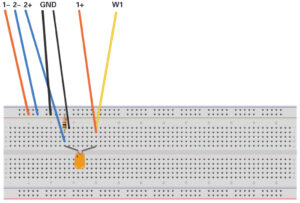
Figure 3. Step 1 setup to measure Cm.
Procedure step 1
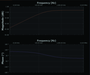
Figure 4. Scopy screenshot.
We chose C1 to be sufficiently larger than Cstray such that we can ignore Cstray in our calculations but still have a similar value to our unknown Cm.
Open the saved data file in a spreadsheet program and scroll to near the end of the data at high frequencies (>1MHz) where the attenuation level is essentially flat. Write down the magnitude; this is GHF1 (in dB). Since we now know GHF1 and C1, we can use the following equation to calculate Cm. Write down your Cm value which we will need when we move to the next step and measure the capacitance of various diode PN junctions.
![]()
Directions step 2
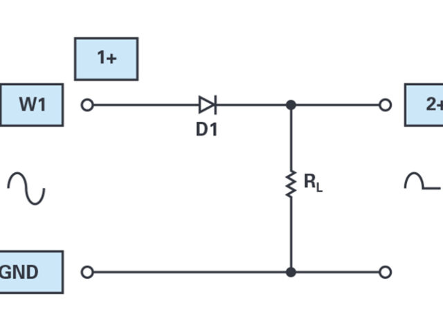
Now we will measure the capacitance of the various diodes from the ADALM2000 analogue parts kit under a range of reverse bias conditions. Build the test setup as shown in Figure 4 and Figure 5 on your solderless bread board. Simply replace C1 with D1, a 1N4001. Be sure to insert the diode with the correct polarity such that a positive offset in AWG1 will reverse bias the diode.
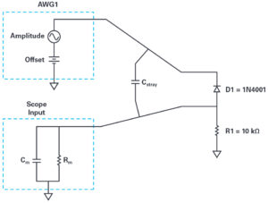
Figure 5. Step 2 setup to measure diode capacitance.
Hardware setup
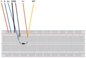
Figure 6. Step 2 setup to measure diode capacitance.
Using the network analyser instrument in the Scopy software obtain a gain (attenuation) vs. frequency plot from 5kHz to 10MHz for each AWG 1 DC offset value in Table 1. Export the data for each sweep to a different .csv file.
Procedure
Fill in the rest of Table 1 with the GHF value for each offset voltage value and using the value for Cm and the equation from Step 1, calculate the value for Cdiode.
Table 1. Capacitance vs. Voltage Data
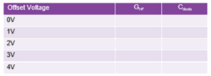
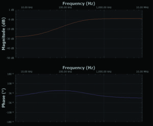
Figure 7. Scopy shot with offset at 0V.
Replace the 1N4001 diode with the 1N3064 diode from the ADALM2000 kit and repeat the same set of sweeps you just did for the first diode. Fill out another table with your measured data and calculated Cdiode values. How do the 1N3064 values compare to those for the 1N4001 diode? You should include a plot of the diode capacitance vs. reverse bias voltage for each diode you measure.
Next replace the 1N3064 diode with one of the 1N914 diodes from the ADALM2000 kit. Again repeat the same set of sweeps you just did for the other diodes. Fill out another table with your measured data and calculated Cdiode values. How do the 1N914 values compare to those for the 1N4001 and 1N3064 diodes?
The capacitance you measure for the 1N914 diode should be much smaller than the other two diodes. It might be small enough to be comparable in size to Cstray.
Extra credit measurements
Light emitting diodes or LEDs are also PN junctions. They are fabricated from materials other than silicon so their turn-on voltage is much different from normal diodes. However, they still have a depletion layer and capacitance. For extra credit, measure the red, yellow, and green LEDs supplied in the ADALM2000 analogue parts kits as you did the normal diodes. Be sure to insert the LEDs into the test setup with the proper polarity for reverse bias. If you did it wrong, you will probably see the LED light up at some point.
Questions
Using the formula given at Step 1, the value of C1, and the plot presented in Figure 4, compute scope input capacitance Cm.
Find the answers on the StudentZone blog page on the Analog Devices website, here.