After the introduction of the SMU ADALM1000 lets continue with the ninth part of the series with some small, basic measurements.
By Doug Mercer and Antoniu Miclaus, Analog Devices
Objective: In this lab activity you will determine real, reactive, and apparent power in RC, RL, and RLC circuits. You will also determine the amount of capacitance that is required to correct the power factor in a series RL circuit.
Background: For time varying voltages and currents, the power delivered to a given load also varies with time. This time, varying power is called instantaneous power. The power at any instant in time can be either positive or negative. That is to say, power is going into the load and being dissipated as heat or stored in the load as energy when positive and coming out of the load (from the stored energy in the load) when negative. The real (or actual) power delivered to the load is the average value of the instantaneous power.
For ac sinusoidal voltages and currents, the real power (P), in units of watts, dissipated in an RC, RL, or RLC load circuit is dissipated in only the resistance part. There is no real power dissipated in an ideal reactive element like a capacitor or inductor. In a reactive element, energy is stored during half of the ac cycle and released (sourced) during the other half of the cycle. The power in a reactive element is referred to as reactive power (Q) and has the units of var (volt-ampere reactive).
The real power (P) dissipated in a load can be calculated as follows:
Where R is the resistive part of the load and I is the (true) rms current.
The reactive power in a load can be calculated as follows:
Where X is the reactance of the load and I is the ac rms current.
When a load has an ac rms voltage (V) across it and an ac rms current (I) through it, the apparent power (S) is the product of the rms voltage and rms current in volt-amperes (VA). The apparent power can be calculated as follows:
If the load has both resistive and reactive parts, apparent power represents neither real power nor reactive power. It is called apparent power because it uses the same equation as dc power but does not take into account the possible phase difference between the voltage and current waveforms.
A power triangle (vector diagram) can be drawn using the real, reactive, and apparent power. The real power is along the horizontal axis, the reactive power is along the vertical axis, and the apparent power forms the hypotenuse of the triangle as shown in Figure 1.

Using geometry, S can be calculated by:
The cosine of angle θ is defined as the power factor (pf). The power factor is the ratio of the real power (P) to the apparent power (S) and is calculated as follows:
Where θ is the phase difference between the voltage waveform (across the load) and the current waveform (through the load). The power factor is thought of as lagging when the load current lags the load voltage (inductive) and leading when the load current leads the load voltage (capacitive).
The real power can also be found from the apparent power by multiplying the apparent power by the power factor:
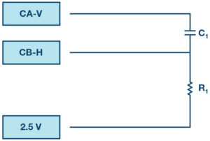
The reactive power in an RC circuit, as in Figure 2, can be calculated using:
Where VC is the rms voltage across the capacitor, I is the rms capacitor current, and XC is the capacitive reactance.
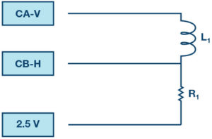
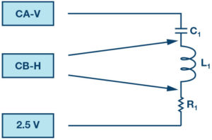
The reactive power in an RL circuit, as in Figure 3, can be calculated using:
Where VL is the rms voltage across the inductor, I is the rms inductor current, and XL is the inductive reactance.
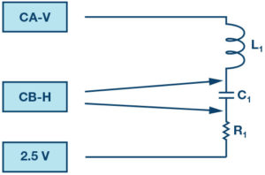
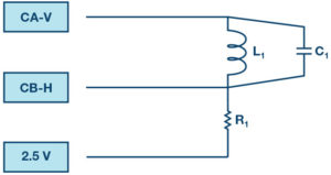
The reactive power in an RLC circuit, as in Figure 4, can be calculated using:
Where VX = VC – VL is the rms voltage across the combined total reactance, I is the rms current in the reactance, and X = XC – XL is the combined total reactance. The rms voltage across the total reactance is equal to the difference between the capacitor voltage (VC) and the inductor voltage (VL), because the voltages have a 180° phase difference (out of phase) between each other.
Power factor correction
Power factor correction is generally required for inductive loads like large ac motors. Because a power factor of 1 (unity) requires less peak current, it is advantageous to compensate for the inductance bringing the power factor as close to unity as possible. By doing this we make the real power close to being equal to the apparent power (VI). Power factor is corrected by connecting a capacitor in parallel with the inductive load.
To find the correct capacitor value required (Figure 5), first we need to know the reactive power of the original RL circuit. This is done by drawing the power triangle and solving for the reactive power. The power triangle can be drawn from the real power and the apparent power and the power factor angle, θ. Once the reactive power for the original load circuit has been found, the capacitive reactance, XC, needed to correct the power factor can be calculated as follows:
Where V is the rms voltage across the RL circuit. Rearranging …
… with a value for XC, the required capacitance can be found based on the frequency (F) as follows:
Rearranging:
With the correct capacitor connected in parallel with the RL load (motor), the power factor will be close to unity—that is, the voltage and current are in phase with each other. And the real power will be nearly equal to the apparent power.
Materials
- ADALM1000 hardware module
- Solderless breadboard and jumper wires
- One 47 Ω resistor
- One 100 Ω resistor
- One 10 μF capacitor
- One 47 mH inductor
Directions for the RC circuit
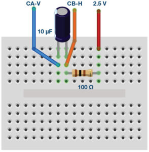
Construct the RC circuit shown in Figure 2 on your solderless breadboard with the component values R1 = 100 Ω and C1 = 10 μF. Three connections to the ALM1000 are required as shown by the green boxes. Open the ALICE oscilloscope software.
Procedure
On the right-hand side of the main scope window, enter 2.5 for the CA-V and CB-V offset adjustment. In this experiment we need to apply ac signals (±voltage) across the load and we are referencing all the measurements to the 2.5 V common rail. Also enter 0 for the CH-A and CH-B vertical position settings (along bottom of scope window). The vertical scales should now be centered on 0 and go from –2.5 to +2.5. Set the CA-I vertical scale to 5 mA/Div.
Set the Channel A AWG Min value to 1.08 V and the max value to 3.92 V to apply a 2.84 V p-p, 1 V rms sine wave centered on 2.5 V as the input voltage to the circuit. Set the frequency to 250 Hz and the phase to 90°. From the AWG A Mode drop-down menu, select SVMI mode. From the AWG A Shape drop-down menu, select Sine. From the AWG B Mode drop-down menu, select Hi-Z mode.
From the ALICE Curves drop-down menu, select CA-V, CA-I, and CB-V for display. From the Trigger drop-down menu, select CA-V and Auto Level.
This configuration uses the oscilloscope to look at the ac voltage and current signals driving the circuit on Channel A and the voltage across the resistance on Channel B. The voltage across the capacitor is simply the difference between Channel A and Channel B (select CAV – CBV from the Math drop-down menu). Make sure you have checked the Sync AWG selector.
The software can calculate the rms values for the Channel A voltage and current waveforms, as well as the Channel B voltage waveform. In addition, the software also calculates the rms value of the point-by-point difference between the Channel A and Channel B voltage waveforms. In this experiment this will be the rms value of the voltage across the capacitor. To display these values, select RMS and CA-CB RMS under -CA-V- and RMS under the -CA-I- sections of the Meas CA drop-down menu. Select RMS under -CB-V- section of the Meas CB drop-down menu. You may also wish to display the max (or positive peak) values for CA-V, CA-I, and CB-V.
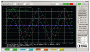
Click on the Run button. Adjust the time base until you have more than two cycles of the sine wave on the display grid. Set the Hold Off to 4.0 ms. You should see four traces: the Channel A voltage, Channel B voltage, Channel A current, and CA-CB voltage Math trace. Because 100 Ω was chosen for the resistor and the vertical scale for the current is 5 mA/Div, the trace of the current in the resistor will fall right on top of the trace for voltage across the resistor, Channel B, with its vertical scale set to 0.5 V/Div (0.5 mA time 100 Ω = 0.5 V).
Record the rms value for the voltage across the total RC circuit (CHA V RMS), the rms value for the current through R1, which is also the current in Channel A in this series circuit (CHA I RMS), the rms value for the voltage across the resistor (CHB V RMS), and the rms value for the voltage across the capacitor (A-B RMS).
Based on these values, calculate the real power (P) for the RC circuit. Calculate the reactive power (Q). Calculate the apparent power (S).
Based on your calculated values for P, Q, and S, draw the power triangle, as in Figure 1. Determine the power factor (pf) and θ for the RC circuit.
The oscilloscope traces are displaying the time relationship between the voltage (the green Channel A voltage trace) and current (the cyan Channel A current trace). Using the display markers or the time cursor, measure the time difference between the zero crossings of the two traces and, from that, the phase angle between them. Use this angle (θ) to calculate the power factor.
How does this compare to the value you obtained from the P, Q, and S and the power triangle? Is the power factor lagging or leading and why?
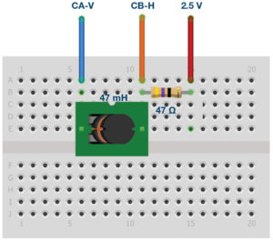
Directions for the RL circuit
First measure the dc resistance of the 47 mH inductor using the dc ohmmeter tool in ALICE. The total series resistance of the RL circuit will be the inductor resistance plus the 47 Ω external resistor R1. The total resistance will need to be factored into your calculations for the real and reactive power.
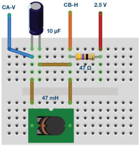
Construct the RL circuit shown in figure 5 on your solderless breadboard with the component values R1 = 47 Ω and L1 = 47 mH.
Procedure
Click on the Run button. Adjust the time base until you have more than two cycles of the sine wave on the display grid. Set the Hold Off to 4.0 ms. You should see four traces: the Channel A voltage, Channel B voltage, Channel A current, and CA-CB voltage Math trace.
Record the rms value for the voltage across the total RL circuit (CHA V RMS), the rms value for the current through R1, which is also the current in channel A in this series circuit (CHA I RMS), the rms value for the voltage across the resistor (CHB V RMS), and the rms value for the voltage across the inductor (A-B RMS).
Based on these values, calculate the real power (P) for the RL circuit. Calculate the reactive power (Q). Calculate the apparent power (S).
Based on your calculated values for P, Q, and S, draw the power triangle, as in Figure 1. Determine the power factor (pf) and θ for the RL circuit.
The oscilloscope traces are displaying the time relationship between the voltage (the green Channel A voltage trace) and current (cyan channel A current trace). Using the display markers or time cursor measure the time difference between the zero crossings of the two traces and from that the phase angle between them. Use this angle (θ) to calculate the power factor.
How does this compare to the value you obtained from the P, Q, and S and the power triangle? Is the power factor lagging or leading and why?
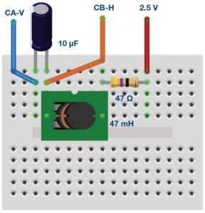
Directions for the RLC circuit
Construct the RLC circuit shown in Figure 7(a) on your solderless breadboard with the component values R1 = 47 Ω, C1 = 10 μF, and L1 = 47 mH.
Procedure
For the RLC circuit you will need measurements for the ac rms voltage across each element. In the configuration shown in Figure 7(a), with Channel B connected to the junction of C1 and L1, we can get the rms voltage across C1 from the difference between the CA and CB waveforms. With Channel B connected to the junction of L1 and R1, we can get the rms voltage across R1 directly from the CB waveform. Record the rms value for the voltage across the total RLC circuit (CHA V RMS), the rms value for the current through R1, which is also the current in Channel A in this series circuit (CHA I RMS), the rms value for the voltage across the resistor (CHB V RMS) and the rms value for the voltage across the capacitor (A-B RMS) when CHB is connected to the junction of C1 and L1 and the combined reactance of L1 and C1 when CHB is connected to the junction of L1 and R1.
We still need the rms voltage across the inductor L1. By swapping the order of the components in this series connected circuit, as shown in Figure 7(c), we do not change the total overall impedance of the load circuit. However, we can now obtain the rms voltage across L1 from the difference between the CA and CB waveforms as we did with the capacitor in Figure 7(a). Record the rms value for the voltage across the total RLC circuit (CHA V RMS), the rms value for the current through R1, which is also the current in Channel A in this series circuit (CHA I RMS), the rms value for the voltage across the resistor (CHB V RMS), and the rms value for the voltage across the inductor (A-B RMS). Check that the value across the total circuit as well as the current through the load and the value across R1 is the same as what was measure for Figure 7(a). Why is this true?
Based on these values calculate the real power (P) for the RLC circuit. Calculate the reactive power (Q) for the combined LC reactance and the L and C individually. Calculate the apparent power (S).
Increase the frequency of Channel A from 250 Hz to 500 Hz and remeasure the rms voltages for the RLC circuit. How has that changed the real, reactive, and apparent power? Is the load current lagging or leading and why?
Decrease the frequency of Channel A from to 125 Hz and remeasure the rms voltages for the RLC circuit. How has that changed the real, reactive, and apparent power? Is the load current lagging or leading and why?
Directions for power factor correction
The circuit shown in Figure 8 for the power factor correction exercise is the same as Figure 6 with the addition of capacitor C1 in parallel with L1.
Based on your measurements from Figure 5 and the equations in the power factor correction section in the background information for this lab activity, calculate the appropriate value for C1 at 250 Hz. Use the closest standard value (or parallel combination of standard values) capacitor for C1.
Procedure
As you did for the simple RL circuit record the rms value for the voltage across the total RL circuit (CHA V RMS), the rms value for the current through R1, which is also the current in Channel A in this series circuit (CHA I RMS), the rms value for the voltage across the resistor (CHB V RMS), and the rms value for the voltage across the inductor (A-B RMS).
Based on these values, calculate the real power (P) for the RL circuit. Calculate the reactive power (Q). Calculate the apparent power (S).
Based on your calculated values for P, Q, and S, draw the power triangle, as in Figure 1. Determine the power factor (pf) and θ for the pf corrected RL circuit. Compare this pf to the one you calculated for just the RL load circuit. How close was the calculated capacitor value to the optimal value needed to make the pf equal to unity? Explain any differences.
Appendix
Using other component values
It is possible to substitute other component values in cases where the specified values are not readily available. The reactance of a component (XC or XL) scales with frequency. For example, if 4.7 mH inductors are available rather than the 47 mH called for, all that is needed to do is increase the test frequency from 250 Hz to 2.5 kHz. The same would be true when substituting a 1.0 μF capacitor for the 10.0 μF capacitor specified.
Using the RLC impedance meter tool
ALICE desktop includes an impedance analyzer/RLC meter that can be used to measure the series resistance (R) and reactance (X). As part of this lab activity it might be informative to use this tool to measure the components R, L, and C used to confirm your test results.
Questions
- In general, which is the effect of improving the power factor?
- Which is the most common way of improving it?
Notes
As in all the ALM labs, we use the following terminology when referring to the connections to the ALM1000 connector and configuring the hardware. The green shaded rectangles indicate connections to the ADALM1000 analog I/O connector. The analog I/O channel pins are referred to as CA and CB. When configured to force voltage/measure current, –V is added (as in CA-V) or when configured to force current/measure voltage, –I is added (as in CA-I). When a channel is configured in the high impedance mode to only measure voltage, –H is added (as in CA-H).
Scope traces are similarly referred to by channel and voltage/current, such as CA-V and CB-V for the voltage waveforms, and CA-I and CB-I for the current waveforms.
We are using the ALICE Rev 1.1 software for those examples here. File: alice-desktop-1.1-setup.zip.
The ALICE desktop software provides the following functions:
- A 2-channel oscilloscope for time domain display and analysis of voltage and current
- The 2-channel arbitrary waveform generator (AWG) controls.
- The X and Y display for plotting captured voltage and current vs. voltage and current data, as well as voltage waveform histograms.
- The 2-channel spectrum analyzer for frequency domain display and analysis of voltage waveforms.
- The Bode plotter and network analyzer with built-in sweep generator.
- An impedance analyzer for analyzing complex RLC networks and as an RLC meter and vector
- A dc ohmmeter measures unknown resistance with respect to known external resistor or known internal 50 Ω.
- Board self-calibration using the AD584 precision 2.5 V reference from the ADALP2000 analog parts kit.
- ALICE M1K voltmeter.
- ALICE M1K meter source.
- ALICE M1K desktop tool.