After the introduction of the SMU ADALM1000 lets continue with the eleventh part of the series with some small, basic measurements.
Written by Doug Mercer and Antoniu Miclaus, Analog Devices
The goal of this lab activity is to examine the issue of capacitive loading of resistive voltage dividers and the resulting effects on frequency response.
Background:
A frequency compensated voltage divider or attenuator is a simple two-port RC network providing a fixed voltage division ratio or attenuation over a wide frequency range and not just at dc. Such networks are used where the part of the circuit loading the voltage divider output is capacitive. This is particularly important when the signal has a wide bandwidth—that is, it is not sinusoidal.
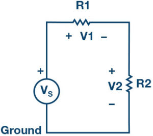
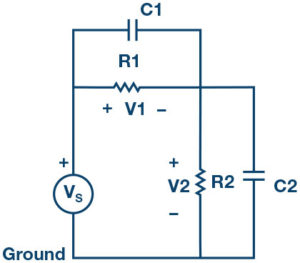
The simplest voltage attenuator is a purely resistive voltage divider with transfer function: H(jω) = V2/VS = R2/(R1 + R2) where the input is VS = V1 + V2, and the output is V2, as in Figure 1. The transfer function of a resistive voltage divider is independent of frequency only if the resistors are ideal and any parasitic capacitances associated with the circuit are negligibly small.
A problem seen at high frequencies is that stray (parasitic) capacitance effects with the overall response of a resistive voltage divider. The simplest way to correct for this problem is to introduce capacitors in parallel to the resistors. Consider the divider circuit in Figure 2. Capacitor C2, which is across the output V2, can be thought of as any stray parasitic capacitance at the output of the divider that might be part of the system.
We can see that this circuit, known as a frequency compensated divider, works like a resistive voltage divider at dc or low frequencies and like a capacitive voltage divider at high frequencies. Voltage dividers can be constructed from reactive components just as they can be constructed from resistors. Also, as with resistor dividers, the divider ratio of a capacitive voltage divider is not affected by changes in the signal frequency even though the capacitor reactance is frequency dependent.
The divider ratio is V2/VS = XC2/(XC1 + XC2). The capacitive reactance XC is proportional to 1/C so V2/VS = C1/(C1 + C2) is similar to the formula for the resistor divider. For the simple case where R1 = R2 we have a divider ratio of ½ for the resistors. To have the same ½ divider ratio for the capacitors, then C1 must be equal to C2.
The compensated divider employs pole-zero cancellation to suppress undesired frequency dependence caused by any stray capacitance on the output side of the network. If the resistor and capacitor values are adjusted so that the pole and the zero of H(s) are superimposed, |H(jω)| becomes independent of frequency.
An instructive way to learn about the conditions for pole-zero cancellation is to write down the low and high frequency limiting expressions for |H(jω)| and then to set them equal to each other. The result is a simple relationship between R1, R2, C1, and C2.
Experiment to compensate for the input capacitance of the ALM1000:
Materials
- One ADALM1000 hardware module
- One 1MΩ resistor
- One capacitor, value to be determined
Directions
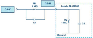
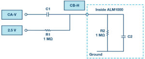
Referring back to Figure 2, we can consider R2 to represent the 1MΩ input resistance of the ALM1000 channels when in Hi-Z mode. Likewise, C2 can be considered to represent the stray parasitic capacitance of the inputs. The resistor and capacitor inside the green box shown in Figure 4. Use another 1 MΩ as R1 to make a ½ divider ratio. Start without including C1 to measure the effect on the frequency response due to C2.
Procedure
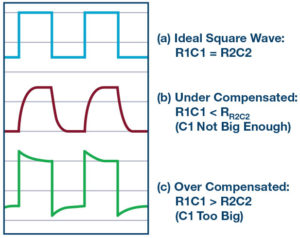
Set AWG A to SVMI mode with the Min value set to 1.0 and Max value to 4.0. Set Shape to Square and the Frequency to 500Hz. Set AWG B to Hi-Z mode. Under Curves, select CA-V and CB-V to be displayed. Hit Run and adjust the horizontal time scale such that about three cycles are visible. You should see a sharp square wave on Channel A and the waveform on Channel B should look like the red curve (b) in Figure 3. This is because C1 has not yet been included. Estimate the RC time constant and the value of C2 from the Channel B waveform.
Open the Bode Plotting window. You can disable the time plot if you would like while generating the frequency response curves. Set the AWG A Min value to 1.082 and the Max value to 3.92 (1Vrms or 0dBV). Check that the shape has been changed to Sine. Set the start frequency to 100 and the stop frequency to 20,000. Select CH-A as the sweep source. Under Curves, select the CA-dBV, CB-dBV, and CA-dB – CB-dB traces to be displayed. Under the FFT window, using the Flat-Top window option works the best. Set the number of sweep point to 300 and single sweep. Hit the Run button.
You should now have the gain (attenuation) ratio vs. frequency response for the uncompensated divider. From the –3 dB point of the gain plot, estimate the RC time constant and the value of C2. How do these values compare to what you calculated using the time domain response? Based on your best estimates for the value of C2, calculate a value for C1 that will exactly compensate for C2. The value you come up with will probably not be close to a standard capacitor value. Find a parallel combination (or series combination) of two or more capacitors that closely adds up to the required value for C1.
Add your new C1 combination across R1 on the breadboard.
Repeat the time domain and frequency domain tests on this new circuit. Does the time domain response of the output of the divider now more closely resemble the blue waveform of (a) in Figure 3? If not, why not? Compare the frequency response of the circuit before and after C1 is added. What is the –3 dB frequency now?
Capacitor divider path response:
Let’s now take a look at just the capacitor divider path. Disconnect R1 from the end of C1 and connect it to the 2.5 V fixed supply as shown in Figure 6. The path through just C1 blocks the dc path from Channel A. Connecting R1 to the fixed 2.5 V supply restores the dc voltage level at the Channel B input.
Repeat the time domain and frequency domain tests on this version of the circuit. Compare the time and frequency domain response of the circuit to what you obtained with just R1 and with R1 and C1 connected in parallel (Figure 5). What is the –3 dB frequency now? Is the frequency response flat, low-pass, or high-pass? Explain why.
Using your divider to measure a 9V battery:
We will now use the voltage divider to measure voltages larger than the 0V to 5V allowed by the ALM1000 hardware. But first we need to calibrate the divider offset and gain.
Disconnect the end of R1 and C1 from Channel A, as shown in Figure 4, and connect them to ground. Set the value for the Channel B gain to 2.0, the approximate divider ratio, for the moment. While monitoring the dc average of Channel B, adjust the value entered in the Channel B offset entry window.
Now reconnect R1/C1 back to the Channel A output. The Channel A and B waveforms should now more closely align on top of each other. Adjust the gain value up or down slightly as needed such that the flat portions of the top and bottom of the square waves are right on top of each other. You might need to tweak the offset slightly as well to get perfect alignment. The software is now calibrated to the voltage divider.
Disconnect R1/C1 from Channel A. Connect the negative (–) terminal of the 9 V battery to ground and connect the positive (+) terminal to R1/C1. The dc average read by Channel B should now be the dc voltage of the 9 V battery. You will need to change the Channel B vertical range to 1 V/div and the position to 5.0 to see the 9 volts on the scope grid.
Oscilloscope probes:
A 10× passive oscilloscope probe uses a series resistor (9MΩ) to provide a 10:1 attenuation when it is used with the 1MΩ input impedance of the scope itself. A 1MΩ impedance is standard for most oscilloscope inputs. This enables scope probes to be interchanged between oscilloscopes from different manufacturers. Figure 6 is the schematic for a typical 10× probe. 10× oscilloscope probes also allow some amount of frequency compensation to allow for variations in the scope channel input capacitance. A capacitor divider network is designed into the probe as shown. The adjustable capacitor connected to ground can then be used to equalize the frequency response of the probe.
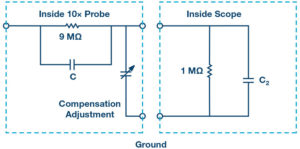
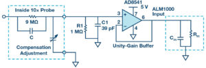
The input channels of the ALM1000 have a 1MΩ input resistance but the input capacitance is much larger than the roughly 10pF to 50pF adjustment range of most 10× probes. The capacitor in parallel with the 9MΩ resistor is typically 10pF and the parallel combination of the scope input capacitance and the adjustable compensation capacitor in the probe needs to be close to 90pF. This means that if a standard probe were connected directly to the ALM1000 input, then it is not possible to compensate the frequency response.
A unity-gain buffer amplifier (such as AD8541 or AD8542) can be inserted between the probe circuit and the ALM1000 input, as shown in Figure 8. R1 and C1 complete the resistor/capacitor divider circuit of the 10× probe.
Questions
Considering the typical probe schematic presented in Figure 8, determine how the adjustable capacitor value can be computed to compensate the frequency response.
Notes
As in all the ALM labs, we use the following terminology when referring to the connections to the ALM1000 connector and configuring the hardware. The green shaded rectangles indicate connections to the ADALM1000 analogue I/O connector. The analogue I/O channel pins are referred to as CA and CB. When configured to force voltage/measure current, -V is added (as in CA-V) or when configured to force current/measure voltage, -I is added (as in CA-I). When a channel is configured in the high impedance mode to only measure voltage, -H is added (as in CA-H).
Scope traces are similarly referred to by channel and voltage/current, such as CA-V and CB-V for the voltage waveforms, and CA-I and CB-I for the current waveforms.
We are using the ALICE Rev 1.1 software for those examples here.
File: alice-desktop-1.1-setup.zip. Please download here.
The ALICE Desktop software provides the following functions:
- A 2-channel oscilloscope for time domain display and analysis of voltage and current
- The 2-channel arbitrary waveform generator (AWG) controls.
- The X and Y display for plotting captured voltage and current voltage and current data, as well as voltage waveform histograms.
- The 2-channel spectrum analyser for frequency domain display and analysis of voltage
- The Bode plotter and network analyzer with built-in sweep generator.
- An impedance analyser for analysing complex RLC networks and as an RLC meter and vector
- A dc ohmmeter measures unknown resistance with respect to known external resistor or known internal 50 Ω.
- Board self-calibration using the AD584 precision 2.5V reference from the ADALP2000 analogue parts kit.
- ALICE M1K voltmeter.
- ALICE M1K metre
- ALICE M1K desktop
For more information, please look here.
Note: You need to have the ADALM1000 connected to your PC to use the software.
Doug Mercer received his B.S.E.E. degree from Rensselaer Polytechnic Institute (RPI) in 1977. Since joining Analog Devices in 1977, he has contributed directly or indirectly to more than 30 data converter products, and he holds 13 patents. He was appointed to the position of ADI Fellow in 1995. In 2009, he transitioned from full-time work and has
continued consulting at ADI as a Fellow Emeritus contributing to the Active Learning Program. In 2016 he was named Engineer in Residence within the ECSE department at RPI.
Antoniu Miclaus is a system applications engineer at Analog Devices, where he works on ADI academic programs, as well as embedded software for Circuits from the Lab and QA process management. He started working at Analog Devices in February 2017 in Cluj-Napoca, Romania.
He is currently an M.Sc. student in the software engineering master’s program at Babes-Bolyai University and he has a B.Eng. in electronics and telecommunications from Technical University of Cluj-Napoca.