After the introduction of the SMU ADALM1000 lets continue with the fourteenth part in the series with some small, basic measurements.
Written by Doug Mercer and Antoniu Miclaus, Analog Devices
Objective:
The objective of this lab activity is to explore the changes to the frequency response of simple passive RC low-pass filters when the effect of loading due to second and third cascaded filter sections is taken into account.
Background:
If two passive RC low-pass filters are cascaded, the frequency response of the cascaded low-pass filter is not the product of the two individual first-order RC low pass-filter transfer functions. This is because the ideal single-pole response assumes a zero-source impedance is driving the filter and there is no load on the output; that is, the filter drives an infinite impedance.
However, directly connecting the second filter acts as a load for the first by effectively changing the combined RC time constant. If you try to analyse the cascaded circuit by simply adding phasors, you will soon realise the shortcomings of that simple technique. This is where using circuit simulation software is very helpful.
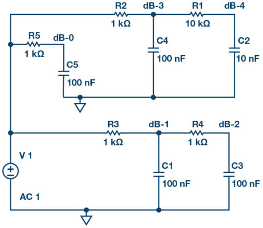
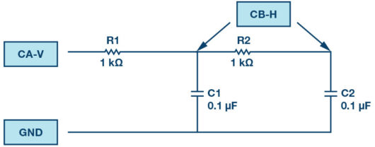
As a prelab exercise, enter the schematic shown in Figure 2 into the ADIsimPE or LTspice circuit simulation, schematic entry software. Three different RC low-pass filter sections are included. The inputs of all three filters are driven by the same ac source V1. Resistor R5 and capacitor C5 form a simple single-pole (first-order) filter with the output taken at node dB-0. Resistors R3 and R4 and capacitors C1 and C3 form a second-order filter with R4 = R3 and C3 = C1.
Two points in this filter should be plotted: the output of the first section at node dB-1 and the output of the second section at node dB-2. Resistors R2 and R1 and capacitors C4 and C2 form another second-order filter with R1 = 10 × R2 and C2 = C4/10. The two similar points in this filter should also be plotted: the output of the first section at node dB-3 and the output of the second section at node dB-4.
This second filter keeps the RC time constant the same for both sections of the filter but reduces the loading effect by increasing the value of the second resistor by a factor of 10 and decreases the value of the second capacitor by a similar factor of 10 (keeping the RC product the same). Using a factor of 10 like this is a good rule of thumb to use when designing cascaded passive RC filters.
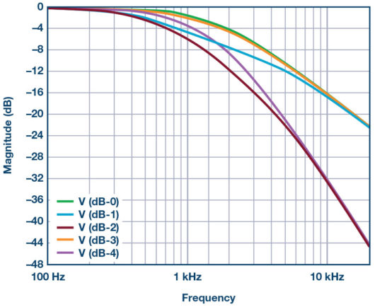
Run the simulation sweeping the input frequency from 100Hz to 20kHz. You should get a frequency response plot that looks something like Figure 3.
A simulation was run sweeping the frequency from 100Hz to 20kHz. As we can see in Figure 3, the completely unloaded first-order filter (dB-0 green line) and the lightly loaded first-order point (dB-3 orange line) are nearly on top of each other. The loaded first-order point (dB-1 blue line) is significantly lower than the other two lines at the frequency of the RC time constant. However, all three converge to the same point at high frequencies, 20kHz.
The two second-order output points at dB-2 (red line, loaded) and dB-4 (pink line, lightly loaded) also show significant differences at the RC time constant frequency but also converge to the same point at 20kHz. At 20kHz the response of the second-order filters are 20dB lower than the first-order filters as one would expect.
Materials:
- ADALM1000 hardware module
- Three 1kΩ resistors
- One 10kΩ resistor
- One 100kΩ resistor
- Three 0.1μF capacitors (marked 104)
- One 0.01μF capacitor (marked 103)
- One 0.001μF capacitor (marked 102)
Directions:
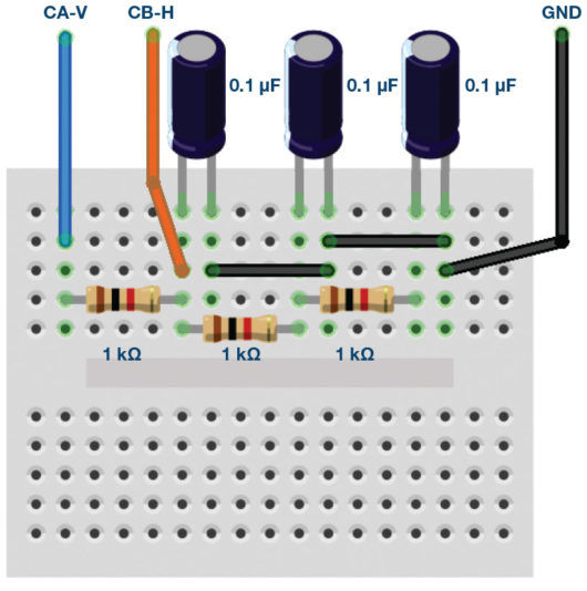
Build the first-order passive RC low-pass filter shown in Figure 3 on your solderless breadboard.
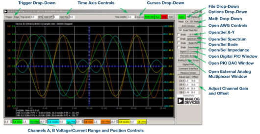
Set up the ALICE desktop Bode Plotter screen as follows. With the bode screen open you can deselect the Enab Time Plot selector and minimise the main scope window.
Set the frequency scale to log.
Under the curves drop-down menu, select CA-dBV (to confirm the input level) and CB-dB – CA-dB (to plot the output response with respect to the input).
Set the start frequency to 100Hz.
Set the stop frequency to 20,000Hz. Select CHA as the sweep source.
Set the number of sweep points to 300. Set the FFT window shape to flat-top.
Under the options drop-down menu, be sure the Cut-DC option is selected.
Use the +dB/div and/or –dB/div buttons to select 5 dB/div on the vertical scale.
Use the LVL+1 and/or LVL-1 buttons to set the level of the top line of the grid to 5dB.
In the AWG controls window, confirm that Channel A is set to SVMI mode and shape sin, and that Channel B is set to Hi-Z mode.
Set the Channel A Min value to 1.0 and the Max value to 4.0.
With single sweep mode selected, click on the green run button. After a few seconds you should have the frequency response plot of the RC filter. Under the options drop-down menu, click on the store trace button to save a copy of the plot. Under the curves drop-down menu, select the saved math plot to be displayed also.
Second-order filter:
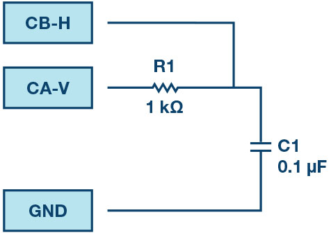
Now add a second RC low-pass section to the filter as shown in Figure 5. The Channel B input will be alternately connected to the top of C1, the output of the first RC section, and the top of C2, the output of the second RC section.
With Channel B connected to the top of C1, click the green start button again. After the new sweep is completed, you should see the saved first-order plot from the first sweep of the filter from Figure 4 and the new live (loaded) first-order plot from the circuit in Figure 5.
Are the two plots the same? If not, explain any differences and why. Use your favourite screen capture method or, under the file drop-down window, click on either the save screen or save data buttons.
Under the options drop-down menu, click on the store trace button to save a copy of the new sweep plot. Now the saved and live plots will be on top of each other.
Move Channel B to the top of C2 and click the green start button again. After the new sweep is completed, you should see the saved first-order plot of the response seen at the top of C1 and the new live second-order response seen at the top of C2. You will want to capture a screenshot of this plot to include in your lab report.
Click on the options drop-down menu and click store trace to save a copy of the new sweep plot.
Change the value of R2 to 10kΩ and the value of C2 to 0.01μF and click the green start button again. After the new sweep is completed you should see the saved second-order plot of the response seen at the top of the 0.1μF C2 capacitor and the new live second-order response seen at the top of the 0.01μF C2 capacitor.
Are the two plots the same? If not, explain any differences and why. You will want to again capture a screenshot of this plot to include in your lab report.
As a way to better understand what is happening due to the changes to R2 and C2, move Channel B back to the top of C1 and click the green start button again. Compare this response curve to the one you observed at the top of C1 when R2 was 1kΩ and C2 was 0.1μF. Explain any difference you observe and why. You will want to capture a screenshot of this plot to include in your lab report.
Third-order filter:
As a further extension of the cascade of the RC low-pass filter sections, add a third RC section to make a third-order filter by connecting R3 and C3 to your circuit, as shown in Figure 5. Follow the same steps you just did on the second-order filter with R1 = R2 = R3 = 1kΩ and C1 = C2 = C3 = 0.1μF. Run a new sweep.
Explain any differences you observe in the frequency responses and be sure to save screenshots along the way to include in your lab report.
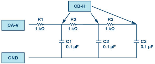
Next, replace your components values as follows: R1 = 1kΩ, R2 = 10kΩ, R3 = 100kΩ and C1 = 0.1μF, C2 = 0.01μF, C3 = 0.001μF.
Run a sweep again.
Questions:
Next, replace your components values as follows: R1 = 1kΩ, R2 = 10kΩ, R3 = 100kΩ and C1 = 0.1μF, C2 = 0.01μF, C3 = 0.001μF.
Run a sweep again.
Notes:
As in all the ALM labs, we use the following terminology when referring to the connections to the ALM1000 connector and configuring the hardware. The green shaded rectangles indicate connections to the ADALM1000 analogue I/O connector. The analogue I/O channel pins are referred to as CA and CB.
When configured to force voltage/measure current, -V is added (as in CA-V) or when configured to force current/measure voltage, -I is added (as in CA-I). When a channel is configured in the high impedance mode to only measure voltage, -H is added (as in CA-H).
Scope traces are similarly referred to by channel and voltage/current, such as CA-V and CB-V for the voltage waveforms, and CA-I and CB-I for the current waveforms.
We are using the ALICE Rev 1.1 software for those examples here. File: alice-desktop-1.1-setup.zip. Please download here.
The ALICE Desktop software provides the following functions:
- A 2-channel oscilloscope for time domain display and analysis of voltage and current
- The 2-channel arbitrary waveform generator (AWG)
- The X and Y display for plotting captured voltage and current voltage and current data, as well as voltage waveform histograms.
- The 2-channel spectrum analyser for frequency domain display and analysis of voltage
- The Bode plotter and network analyser with built-in sweep generator.
- An impedance analyser for analysing complex RLC networks and as an RLC meter and vector
- A dc ohmmeter measures unknown resistance with respect to known external resistor or known internal 50Ω.
- Board self-calibration using the AD584 precision 2.5V reference from the ADALP2000 analogue parts kit.
- ALICE M1K voltmeter.
- ALICE M1K meter
- ALICE M1K desktop
For more information, please look here.
Note: You need to have the ADALM1000 connected to your PC to use the software.
Doug Mercer received his B.S.E.E. degree from Rensselaer Polytechnic Institute (RPI) in 1977. Since joining Analog Devices in 1977, he has contributed directly or indirectly to more than 30 data converter products and he holds 13 patents. He was appointed to the position of ADI Fellow in 1995. In 2009, he transitioned from full-time work and has continued consulting at ADI as a Fellow Emeritus contributing to the Active Learning Program. In 2016 he was named Engineer in Residence within the ECSE department at RPI.
Antoniu Miclaus is a system applications engineer at Analog Devices, where he works on ADI academic programmes, as well as embedded software for Circuits from the Lab and QA process management. He started working at Analog Devices in February 2017 in Cluj-Napoca, Romania. He is currently an MSc student in the software engineering master’s programme at Babes-Bolyai University and he has a B.Eng. in electronics and telecommunications from Technical University of Cluj-Napoca.