

This post tells about how to calculate the delay in VLSI design using RC representation, including the term of transfer function.
Let’s consider the circuit depicted below. This is RC model of inverter.
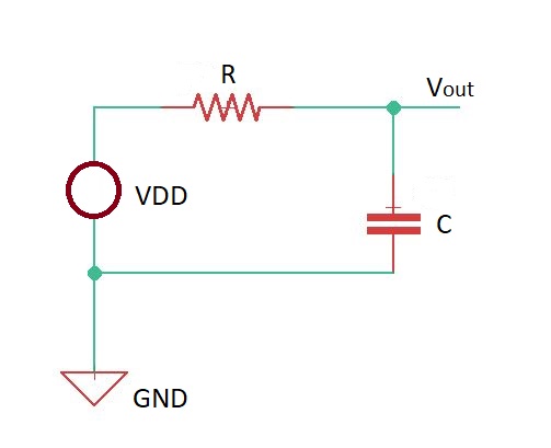
Let’s consider transfer function for the circuit. Transfer function describes behaviour of the output signal, depending on the input signal. Transfer function for this circuit is , step response is . Here is a delay.
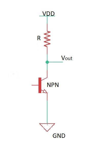
Let’s consider NAND gate (second-order system) below.
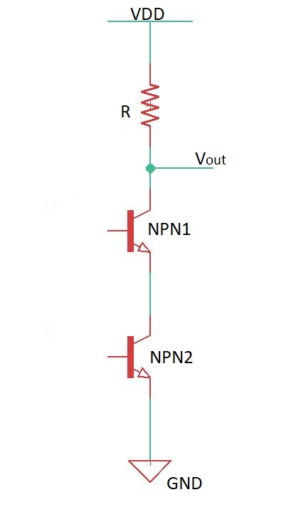
The transfer function here is . The step-response here is , here . Here is a delay.
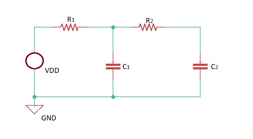
Most of the circuits can be represented as a tree of RC circuits with the voltage source root. So we can conclude that delay in a general circuit is .
Let’s calculate the delay for an inverter driving n identical load inverters like on the drawing below.
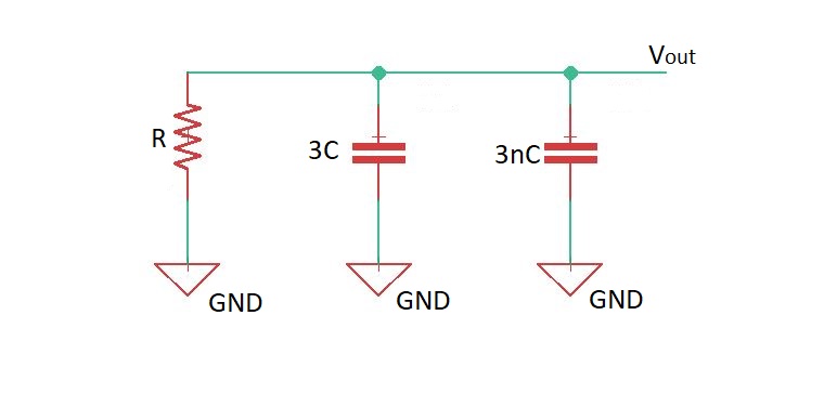
Here load is represented by capacitance , driving inverter is represented by the capacitance . Then the total capacitance is , and the delay is .
Usually it is comfortable to speak about delay in the non-process related terms normalising the delay to parasitic capacitance , so we have .
Educational content can also be reached via Reddit community r/ElectronicsEasy.


