Semiconductor materials contain not only elements, but also chemical compounds. Semiconductors can be organic and non-organic, crystalline and amorphous, solids and liquids. Despite the fact that they are different forms of substance, they all change their properties dramatically in an electromagnetic field.
Silicon and germanium are the most wide spread materials for electronic components production. Practically interesting are also two and three component compounds. We will consider all these semiconductor types below.
Germanium, Ge. Germanium is often met in nature, but it is quite widespread, and can be found in natural minerals in very small quantities. That’s why industrial germanium is usually a by-product of zinc production, coal cooking, and a result of copper-lead-zinc ore processing.
Pure germanium has a metallic sheen, characterised with high hardness and brittleness. Its unit cell has eight atoms, and crystalline lattice is a diamond type. Crystal germanium is stable in the air at room temperature. When heating to 650°C, it creates Ge02 dioxide, and dissolves in water. Germanium does not dissolve in water, or sulfuric or hydrochloric acids. Active germanium solvent is a solution of nitric and hydrofluoric acids. Germanium has low melting temperature and low saturated vapor pressure. It greatly simplifies the process of Ge production.
Electron mobility at a room temperature for germanium is two times bigger than for holes. However, temperature changes its ratio. Electronic components production uses different electrically active impurities. The process of impurities injection in a semiconductor is called alloying. The most frequent materials as donors and acceptors are elements of V and III groups of the periodic system of elements. These impurities create small levels in the forbidden band with the ionisation energy about 0.01eV. Elements of I, II, VI, VI and VIII have very complex behaviour. And they create big energy levels in a forbidden band of Ge – the reason is big valence difference of these elements.
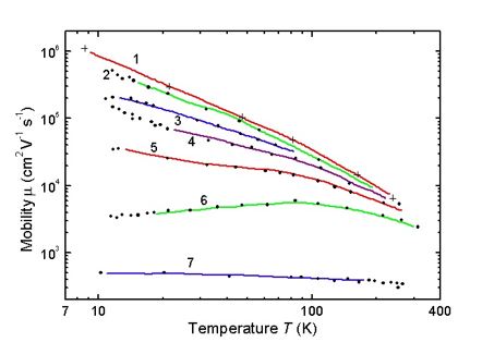
Small donors and acceptors are totally ionised at a temperature higher than 90K, so at room temperature, charge carrier concentration in germanium is determined by impurity concentration. For the low alloyed germanium in the wide range of temperatures, temperature coefficient of resistance has a positive trend. Semiconductor mobility decreases when the temperature rises, because of the charge carrier dissipation on the oscillating atoms of a crystalline lattice. (Figure 24, by Ioffe Saint-Petersburg Institute).
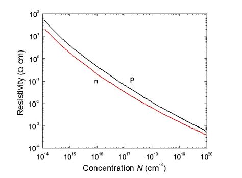
Conductivity and mobility has straight proportional connection. The temperature when intrinsic conductivity occurs for Ge, is determined by impurities concentration. Practical interest has Ge resistivity dependent of impurity concentration, as you can see in Figure 25 (by Ioffe Saint-Petersburg Institute). It can be used for alloying impurity concentration calculations. For resistance the following formula is valid:
Silicon, Si. Si is very widespread in nature, it is 29% by mass, and second place after oxygen. It also has diamond-type crystalline lattice, but is smaller than germanium. There are smaller distances between atoms in a crystalline lattice for Si, and strong covalence bands in a lattice. Si does not dissolve in water and does not react with most acids at room temperature. It can be dissolved only in a solution of nitric and hydrofluoric acids. Si has quite a high melting temperature, and behaves chemically actively in a molting state.
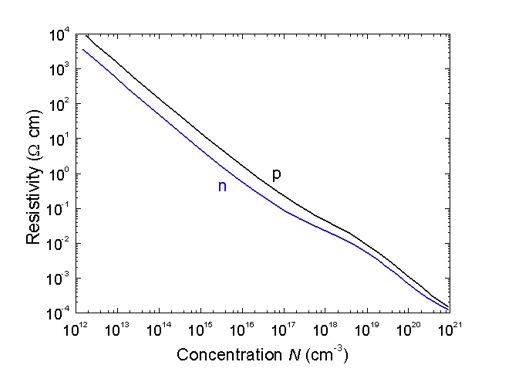
The most frequent compound of Si is SiC – stable compound of Silicon and Carbon, which has strong semiconductor properties. Si has a wider forbidden band then Ge, which is why Si resistivity is much bigger than Ge resistivity. Impurity behaviour in Si are similar to the ones at Ge. III and V group elements create small energy levels in the forbidden band with ionisation energy at 0.05eV. Impurity elements of I, II, VI and VII groups create large energy levels in the forbidden band of Si. The most frequent Si alloying method and method for p-n transition create a method of diffusion of electrically active impurity. Figure 26 shows resistivity dependence of impurities concentration in a Si crystal (by Ioffe Saint-Petersburg Institute).
For Si, small donors diffuse much slower than acceptors. For Ge, reverse, small donors are diffusing much faster than acceptors. The reasons of this difference are deep inside their atomic structure. Vacancies in a crystalline lattice of Si and Ge are acceptors, and they create deep energy levels in the forbidden bands of these elements. For Ge, acceptor level is in the forbidden band, close to the top of valence band. For Si it is close to the bottom of the conduction band. It reflects the impurity diffusion. For Ge, Columb interaction is between impurities and vacancies. For Si, most of vacancies are in a neutral state, so diffusion rate is small. These and some other structural factors are complicating the process of a monocrystals creation.
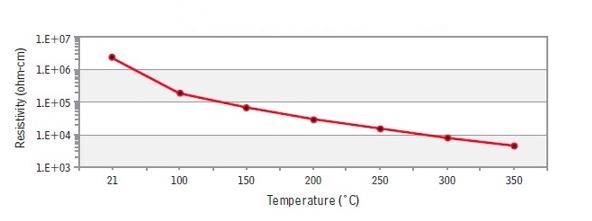
Silicon Carbide, SiC. SiC is only one semiconductor, being a compound of elements of IV group of the periodic table of elements. SiC is characterised by covalent bond, strong chemical and temperature stability and hardness. Hexagonal modification of SiC has a lot of polytyps. Polytypism is a crystallographic term. Polytypism is a characteristic of an element or compound, which occurs in several structural modifications, in accordance to how a compound is build up. All modifications will have identical structure and consistence, but differ with layers stacking in a structure. The most frequent polytyps of SiC are a – and β modifications. All modifications are different with the forbidden band width and electron mobility. Variation of these electrical parameters allow us to consider SiC as a group of semiconductor materials, having the same structure and composition. Here volume resistance versus temperature is provided for HR modification of SiC (by CoorsTek Ink. Materials) in Figure 27.
Polytypism control presents quite a difficult technological challenge. Polytypism depends on temperature, growth rate, type of applying impurities and another factors. SiC electroconductivity is considered by impurities at room temperature. Also, electroconductivity and colour of material are dependent on the domination of Si or C atoms in a crystal. Pure SiC is transparent. Impurities of V group elements (N, P, As, Sb, Bi) in SiC are coloured green and characterised with n-type conductivity. Impurities of III (B, Al, Ga, In) and II (Ca, Mg) group elements are coloured with blue and violet and are characterised with p-type conductivity. Domination of Si atoms in a crystal leads to n-type conductivity, C atoms – to p-type conductivity. Intrinsic conductivity of SiC starts at 1,400°C temperature.
An important feature of a SiC is its ability to luminescence in a visible part of the spectrum. By changing impurities composition in different polytypes of a SiC, any colour luminescence can be achieved in a crystal – from red to violet. At the very beginning, SiC was used as a source for yellow LED production. However, it has low efficiency of transformation of electrical energy to light. So nowadays other materials and techniques are used for producing different colour LEDs. SiC also has very good materials for field transistors and RF components production with proper frequency properties.
Semiconductors A3B5
A3B5 compounds are the closest equivalents of Si and Ge by their electro-physical properties. These compounds are created with elements of III groups of the periodic table (B, Al, Ga, In) and elements of V groups of the periodic table (N, P, As, Sb). The compounds are named for their metalloid ‘roots’ – nitrides, phosphides, arsenides and antimonides. All A3B5 compounds can be crystalised in the zinc-blend cubic type lattice, except nitrides. Nitrides are characterised by hexagonal type lattice. A3B5 compounds are characterised by acceptor-donor bound. From four valence atoms in a lattice structure, three are sharing valence electrons between A3 and B5 atoms. The fourth bond is a bond between B5 atoms.
Charge carrier mobility for A3B5 compounds is limited by charge carrier dissipation on the atom’s optical oscillations of the lattice. Atoms of this crystalline lattice have some ionic charge, which results in dipole creation. It is rising charge carrier dissipation. From another side, the rising of compound atomic mass, decreasing amplitudes of atomic oscillations and decreasing their dissipation, increase charge carrier mobility. Most A3B5 compounds have a simple process of alloying – electron-hole pairs are created quite simply for these compounds. An important feature of A3B5 compounds is their ability of recombination of non-equilibrium charge carriers. For radiation generation in a visible part of spectrum, the forbidden band width for the semiconductor should be not less then 1.7eV. From A3B5 compounds only GaP and GaN are satisfying to this condition. Compounds with a smaller forbidden band can radiate in the infrared part of spectrum, like GaAs. Effective luminescence of GaP and GaN can be achieved after alloying them with impurity elements.
A wide range of forbidden bands of A3B5 compounds allows the creation of photodetectors, covering a wide spectrum range. The most frequent components are photodiods and phthelements. GaAs can be used in solar panels. These compounds can also be used as a microwave oscillator, because of its instability in strong electromagnetic fields. GaAs and InSb can be used for tunnel diode production. Narrowband A3B5 compounds can be used for magnetoresistor and Hall transformer production. Alloyed GaAs is used for production of field transistors and high speed integral circuits.
Semiconductors A2B6
A2B6 compounds are chalcogenides of Zn, Cd anf Hg. They are sulphides, selenides and tellurides. These compounds can be crystalised in the zinc-blend cubic or hexagonal type lattice. Chemical bond is covalent – ionic. A large component of ionic bond in these compounds result in the big width of the forbidden band and low charge carrier mobilities.
Impurity behaviour for A2B6 compounds is the same as for A3B5, when impurities with smaller valence play the role of acceptors, and impurities with bigger valence than solvent atoms play the role of donors. An important feature of compounds is that they demonstrate only one type of conductivity.
The most widely used A2B6 compound are ZnS and CdS. ZnS is the base for luminophore production. CdS is used for production of photoresistors with high sensitivity in the visible part of the spectrum. Luminophore’s radiation spectrum is considered by luminescence activators. The most widely used are copper activated electroluminophors, emitted in the blue and green part of spectrum. The disadvantage of electroluminescence devices is based on ZnS and has a big trend to degradation, because of the strong ionic chemical bond.
Semiconductors A4B6
Among all A4B6 compounds the most studied ones are zinc chalcogenides (PbS, PbSe, PbTe). They can be used as IR detectors, due to their narrow forbidden band. They cristalise in a cubic type lattice. Their chemical bonds have a strong ionic component. An excess of Pb atoms in the compound results in electron type conductivity, excess of chalcogen atoms results in hope type conductivity. The type of conductivity for these compounds can be changed by impurity implementation in the compound structure. I group elements (Na, Cu, Ag) are acceptors. VII group elements are donors, when replacing the Pb atom. Energy levels of impurities are usually coalescing with conductivity or valence band (depending on the type of impurity). A4B6 compounds usually have very big permittivity coefficient. The main application of A4B6 compounds are photodetectors with high spectral sensitivity, and semiconductor laser production.