For semiconductors, as for metals, there will be potential differences on the contacts with different temperatures, and an electrical current will occur between these contacts. Uneven heating of a semiconductor will cause charge carrier energy gradient in its different parts. Temperature change in the semiconductor may also cause changes in charge carrier concentration distribution across the semiconductor.
It causes diffusion flow of charge carriers, from hot to a cold part of a crystal. Internal electric fields prevent further charge carrier division, and cause the equilibrium process in the semiconductor. Both electrons and holes are taking part in the thermo-EMF creation in a semiconductor. And their thermo-EMF components have opposite signs.
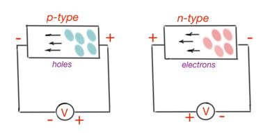
In the n-type semiconductor, the main charge carriers are electrons, and they move from the hot contact to cold contact of semiconductor, creating negative excessive charge on the cold contact. For p-type semiconductors, holes take part at the diffusion process, and the thermo-EMF polarity changes to the opposite – Figure 22. A different reaction of an impurity semiconductor on the heterogenerity of a heating process helps to use thermo-EMF to find out semiconductor type.
Hall effect
Physical phenomena accruing in a semiconductor after application of electric and magnetic field are called galvanomagnetic effects. Hall effect is the most important among all galvanomagnetic effects. Hall effect states that, if we put semiconductor plates with an electrical current onto electromagnetic field, perpendicular to the plate, there is a potential difference that will appear on the sides of the plates with the direction perpendicular to the electromagnetic field, called Hall EMF – Figure 23.
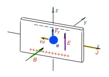
Hall EMF is due to the fact that there is a Lorenz force affecting the charge carriers with the speed v, in the magnetic field , and shifts them to one of the sides of the plate.
Direction of the Lorenz force is determined only by the electric and magnetic field. Holes and electrons will deviate to the same side of a plate. And, for different types of semiconductor, Hall EMF will have a different polarity. Hall EMF helps to find out charge carrier type in a semiconductor, their concentration and charge carrier mobility.
Hall effect for degenerate semiconductors
Lorenz field will stop shift charge carriers, when the equilibrium electric field of the shifted charges are established in the semiconductor. So for this equilibrium:
If the electric field is homogenous, and , and geometry of the plate is the following: , then:
Where is a Hall electric field, is a plate length, is a plate width. This formula helps us to estimate Hall coefficient . For n- and p- type semiconductors, the sign of a Hall coefficient will be different, because of the electric field.
This formula works only for semiconductors where charge carrier speed distribution is not taken into account. However, generally speaking Hall coefficient depends on the charge carriers concentration, and thus the temperature of a semiconductor. Hall coefficients for n- type and p-type semiconductors:
Where . Measuring Hall EMF in some temperature ranges, we can get charge carrier concentration distribution for different temperatures, and it will help to estimate ionisation energy for donors and acceptors, and calculate concentration of electrically active impurity. So for charge mobility we can get the following:
Hall effect for non-degenerate semiconductors
For non-degenerate semiconductors Hall coefficient can be calculated by the following formulae: