The objective of this lab activity is to apply the voltage injection method using the ADALM2000 network analyser and a transformer to measure the loop gain of a negative feedback system such as an inverting op amp gain stage.
Written by Antoniu Miclaus and Doug Mercer, Analog Devices
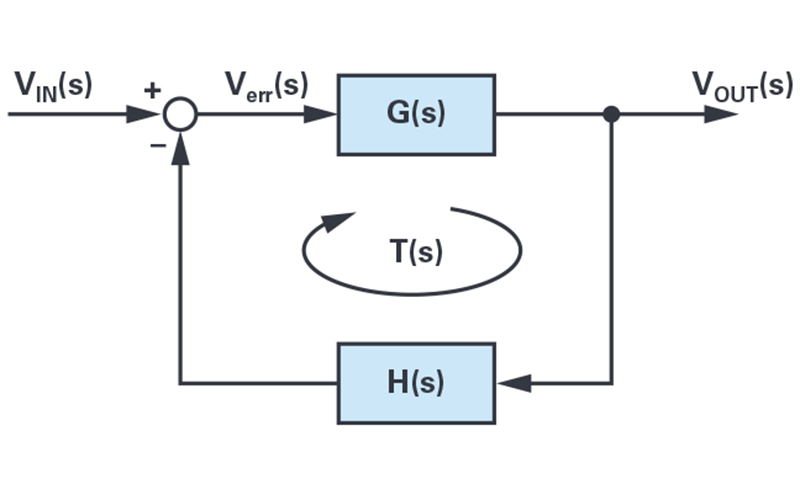
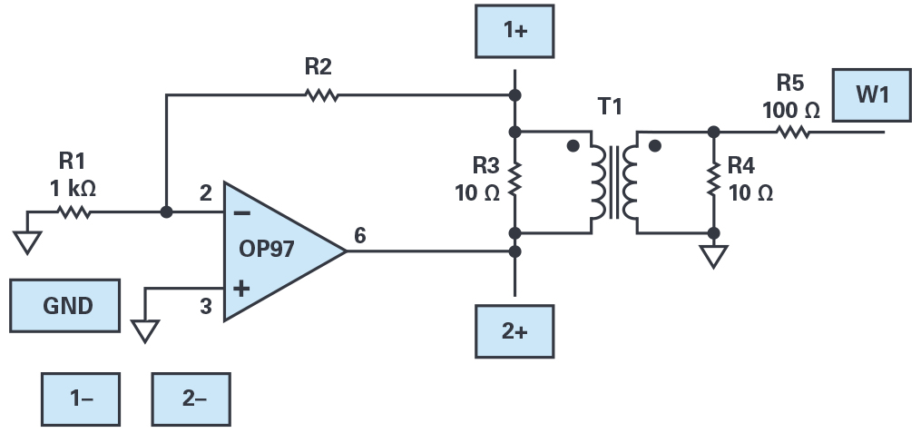
Negative feedback is commonly used in control systems. Figure 1 shows a simple system with negative feedback.
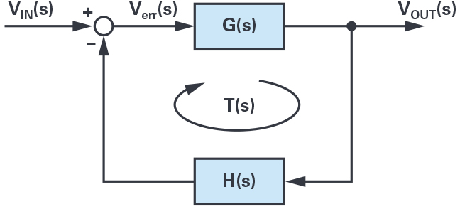
The output voltage is related to the input voltage by:
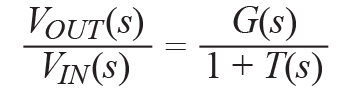
This is the closed-loop transfer function. T(s) is called the loop gain, which is the product of all gains around the loop and is equal in this case to T(s) = G(s) × H(s).
With the loop gain we can apply the Nyquist stability criterion to measure the gain and phase margin and determine the overall stability of the closed-loop system.
The loop gain of a system can be derived from a mathematical model of the system. Such models often do not consider all the parasitics and unwanted effects that might exist in the real system. It can be very useful to measure the loop gain of a negative feedback system during the design process.
Loop gain measurement
One method to measure the loop gain in negative feedback systems is the voltage injection method. The following details show how the voltage injection method can be applied in practice and what has to be considered to achieve correct results.
By using a suitable injection transformer (the ADALP2000 analog parts kit contains an HPH1-1400L), we can inject a test voltage at an appropriate injection point in the feedback loop of the system. Then the response of the loop can be measured using a network analyser like the ADALM2000.
Figure 2 shows a setup using the voltage injection method to measure the loop gain of a feedback system. A low value resistor is inserted in the feedback loop at the injection point. The injection transformer secondary winding is connected across the injection resistor to apply the test voltage. This allows the injection of a test voltage without changing the dc bias operating point of the system.
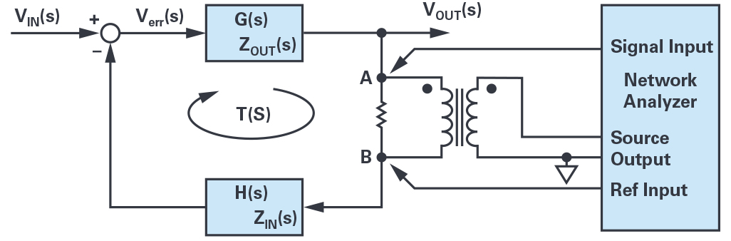
The network analyser inputs are connected to both sides of the injection resistor using voltage probes. The loop gain is then measured by measuring the complex voltage gain from point A to B:
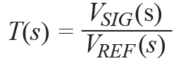
Where T(s) is the measured loop gain and VSIG and VREF are voltages measured by the network analyser.
The measured loop gain T(S) approximately equals the actual loop gain if the following two conditions are met.
Condition 1
The impedance looking forward around the feedback loop (ZIN(s) of block H(s)) is much greater than the impedance looking backward from the injection point (ZOUT(s) of block G(s)).
![]()
Condition 2
The second condition that must be fulfilled to ensure that the measured loop gain equals approximately the real loop gain is:
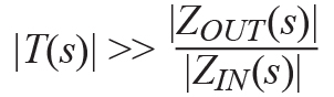
From these conditions we see that it is important to choose a suitable injection point that fulfils both conditions.
The first condition is often fulfilled at the output of an op amp that is normally low impedance. Other suitable points are generally at high impedance inputs like op amp inputs.
The second condition is more difficult to check, especially small loop gain results. When these results are above the crossover frequency, they need to be checked very carefully.
The magnitude of the injection voltage should be kept as low as possible to avoid large signal effects such as saturation or other nonlinearities that will influence the measurement.
The size of the injection resistor does not directly influence the measurement result if it is kept relatively small. 50 Ω or less is a good number.
The frequency response of the transformer and the dynamic range of the network analyser will limit the loop gain measurement. In the following lab setup, you will be using the HPH1-1400L transformer that has a usable frequency response of perhaps 10 kHz to 5 MHz. To measure loop response at lower frequencies, a transformer with much higher winding inductance will be needed. The HPH1-1400L, or similar wideband transformers like a T1-6T (Mini-Circuits) or WB1010 (Coilcraft) should be sufficient to observe the loop response near unity-gain (0 dB) of some of the operational amplifiers supplied in the ADALP2000 analogue parts kit when connected as inverting gain stages with feedback resistor ratios (H(s)).
Materials
- ADALM2000 active learning module
- Solderless breadboard and jumper wire kit
- Two 10 Ω resistors
- One 100 Ω resistor
- Two 1 kΩ resistors
- One 10 kΩ resistor
- One OP27 op amp
- One OP37 op amp
- One OP97 op amp
- One HPH1-1400L transformer (or transformers, such as the T1-6T from Mini-Circuits or WB1010 from Coilcraft)
- Two 0.1 μF capacitors (used to decouple the Vp and Vn power supplies)
Directions
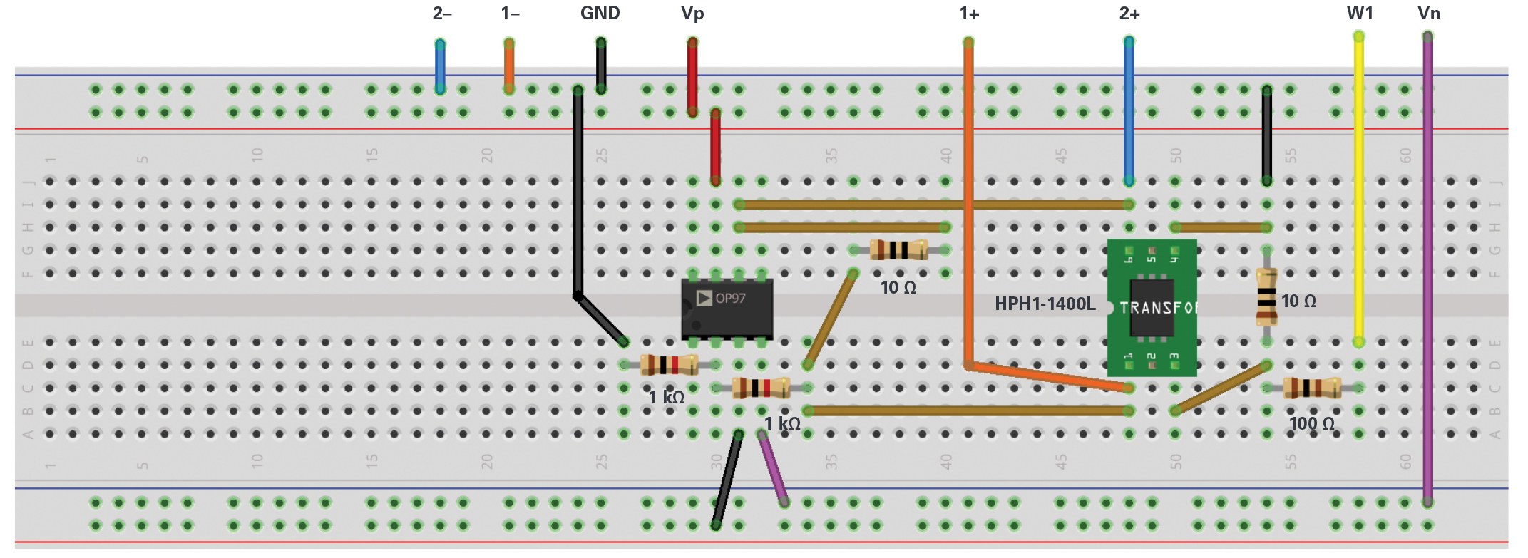
Build the measurement setup as shown in Figure 3. Remember to supply power to the op amp (+5 V to pin 7 and –5 V to pin 4) with 0.1 μF capacitors used to decouple the Vp and Vn power supplies (not shown in the schematic diagram for simplicity). If you are using the HPH1-1400L transformer for T1, you should connect three of the six windings in series for the primary side and the remaining three windings in series for the secondary side (see this activity on transformers for more details). Resistor R1 is set to 1 kΩ and R2 is either 1 kΩ or 10 kΩ to test different loop gains with the three different op amps.
Voltage divider R4 and R5 serves two purposes. First, the 10 Ω R4 matches the impedance of the resistor inserted in feedback loop R3. The AWG in the ADALM2000 cannot directly drive the 10 Ω resistor, so the 100 Ω R5 increases the load resistance to a value high enough for the AWG to safely drive.
Secondly, the attenuation of the divider allows us to set the amplitude of the AWG high enough to provide a low noise signal while still injecting a small signal into the loop.
Hardware setup
The light blue squares indicate where to connect the ADALM2000 module AWG, scope channels, and power supplies. Be sure to turn on the power supplies only after you double check your wiring.
Open the voltage supply control window to turn on the fixed +5 V and –5 V power supplies. Open the network analyser instrument and set the sweep to start at 10 kHz and stop at 5 MHz. The max gain should be set to 1×. Set the amplitude to 3 V and the offset to 0 V. Under the Bode scale, set the magnitude top to 40 dB and the range to 80 dB. Set the phase top to 180° and range to 360°. Under the scope channels, click on Use Channel 1 to use it as a reference. Set the number of steps to 500.
Procedure
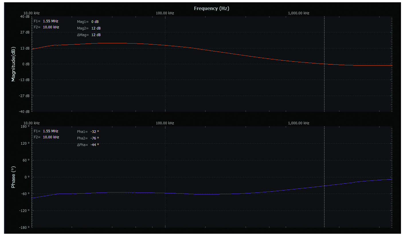
Use the lower bandwidth OP97 amplifier from the ADALP2000 parts kit for your first measurements, with both R1 and R2 equal to 1 kΩ. Turn on the power supplies and run a single sweep. Note the frequency where the loop gain is unity (0 dB) and the phase at that frequency. Be sure to export the sweep data to a .csv file for further analysis in either MATLAB or Excel.
A plot example is presented in Figure 5.
Next replace the OP97 amplifier with the higher bandwidth OP27 amplifier from the parts kit. Be sure to turn off the power supplies before removing the op amp from your circuit. Turn on the power supplies and run a single sweep. Note the new frequency where the loop gain is unity (0 dB) and the phase at that frequency and compare this to the measured result for the OP97. Be sure to export the sweep data to a .csv file for further analysis in either Excel or MATLAB. Now replace R2 with a 10 kΩ resistor. Run a single sweep. Note the new frequency where the loop gain is unity (0 dB) and the phase at that frequency and compare this to the measured result for the OP27 with R2 equal to 1 kΩ.
The final step involves replacing the OP27 amplifier with an OP37 amplifier from the parts kit. Be sure to turn off the power supplies before removing the op amp from your circuit. Turn on the power supplies and run a single sweep. Note the new frequency where the loop gain is unity (0 dB) and the phase at that frequency and compare this to the measured result for the OP27 with R2 equal to 10 kΩ. Be sure to export the sweep data to a .csv file for further analysis in either Excel or MATLAB.
Question:
Taking into consideration the loop gain measurement setup described in Figure 3, what is the purpose of the R2 and R3 in the circuit?
You can find the answer at the StudentZone blog.