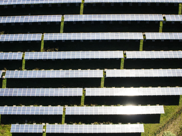
Since the discovery of graphene, two-dimensional materials have been the focus of materials research. Among other things, they could be used to build tiny, high-performance transistors. Researchers at ETH Zurich and EPF Lausanne have now simulated and evaluated one hundred possible materials for this purpose and discovered 13 promising candidates.
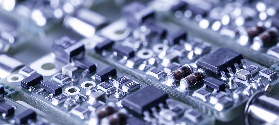
With the increasing miniaturization of electronic components, researchers are struggling with undesirable side effects: In the case of nanometer-scale transistors made of conventional materials such as silicon, quantum effects occur that impair their functionality. One of these quantum effects, for example, is additional leakage currents, i.e. currents that flow “astray” and not via the conductor provided between the source and drain contacts.
It is therefore believed that Moore’s scaling law, which states that the number of integrated circuits per unit area doubles every 12-18 months, will reach its limits in the near future because of the increasing challenges associated with the miniaturisation of their active components. This ultimately means that the currently manufactured silicon-based transistors — called FinFETs and equipping almost every supercomputer — can no longer be made arbitrarily smaller due to quantum effects.
Two-dimensional beacons of hope
However, a new study by researchers at ETH Zurich and EPF Lausanne shows that this problem could be overcome with new two-dimensional (2-D) materials — or at least that is what the simulations they have carried out on the “Piz Daint” supercomputer suggest.
Source: “Simulation microscope” examines transistors of the future”, Simone Ulmer, ETH Zurich News