This post tells about the antenna effect in VLSI and antenna rules in VLSI. During a real manufacturing process some undesirable effects can occur. One of them is so called antenna effect, or plasma-induced gate-oxide damage or plasma-induced damage.
Antenna effect in VLSI implies to the charge collection effect, but not to the device called antenna. significant amount of charge usually induced during the process of plasma etching and other processes.
The principle here is that if conducting material or wire will be connected to the gate of the device, the wire here will act as antenna, inducing significant amount of charge and diodes formed by drain and source diffusion layers can conduct significant amount of current. Finally antenna effect cause gate breakdown or decreasing I-V characteristics.
Problems that can occur:
- changing threshold voltage;
- reduced life expectancy of a device;
- increased gate leakage
In order to avoid problems above, there is antenna rules determined. They are indicating maximum area of metal to connect to a gate, avoiding antenna effect. Depending on the breakthrough voltage of the transistor maximum ratio of the wire area to gate area may vary from 100:1 to 5000:1. Thicker gate of the transistor, higher ratio.
On the figure below you can see a long wire, connected to the gate, forming gate breakthrough. As soon as it is not connected to the diffusion layer, antenna effect happens during plasma etching.
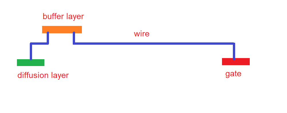
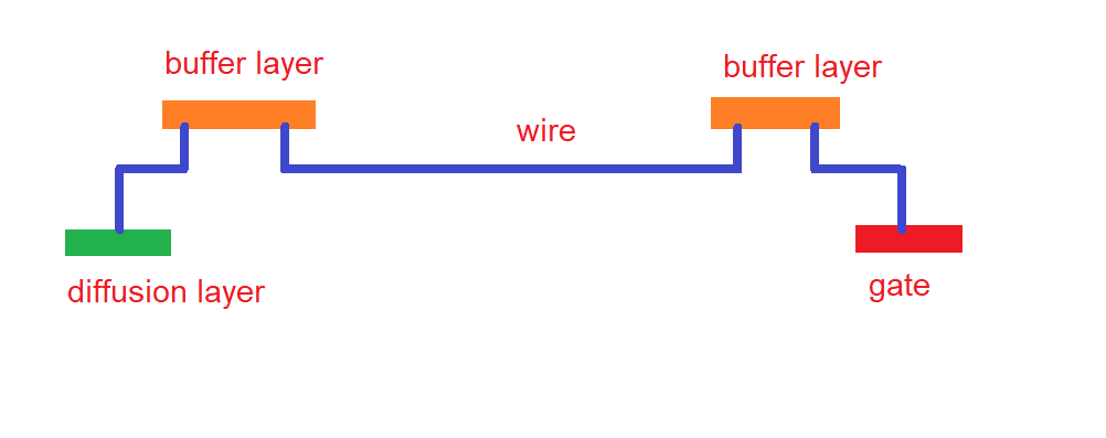
One way to solve the problem is to divide the wire into two parts as shown on the figure below and to connect wire and a gate with the buffer layer.
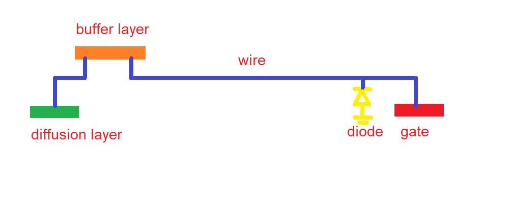
The other way to solve the problem is to connect diode to the wire, to create rout for discharge during the etching process as shown on the figure below.
More educational content can be found at Reddit community r/ElectronicsEasy.