CVD (or Chemical Vapour Deposition) of a solid on a heated surface from a chemical reaction in a vapour phase. This is a process of thin film formation on the atomic level. CVD is a general process, combining a set of processes like PVD, MBE, ion vapour deposition.
CVD processes have many advantages. It is characterised with high deposition rates so the thick layer can be quickly created, it has high throwing power, CVD equipment does not require high vacuum and can be adjusted to different process variations.
The CVD process is flexible for variations of compounds. When the process demands high work temperatures – +600 and above – MOCVD or plasma – CVD processes are in use, as they are more useful in conditions when work materials are not thermally stable. The precursors and by-products of the CVD process are toxic and maybe hazardous.
CVD processes were and still are the subject of research and developments in universities and commercial laboratories, in accordance to growing demands and requirements of the industry. CVD is mostly in use in semiconductor production for microelectronics. The leaders in CVD and PVD equipment are US, Japan and Germany. Asia-Pacific is the largest microelectronics area in the world, followed by North America. [1]
The CVD process combines a few disciplines like thermodynamics, plasma physics, kinetics, fluid dynamics, and chemistry – specifically reactions like pyrolysis, hydrolysis, oxidation, carburisation and nitridation. CVD reaction is run by thermodynamics and kinetics. The first one determines the process direction. The second one, the process rate. If the CVD process of thermodynamics and kinetics is used properly, then the designed layers will be deposited more precisely.
Chemical reactions that occur during the CVD process:
- Pyrolysis or thermal decomposition
- Hydrogen reduction
- Coreduction
- Oxidation
- Hydrolysis
- Carbidisation
- Nitridation
The precursors for the CVD process are halides, carbonyls and hydrides.
As mentioned above, the CVD process has now evolved in the MOCVD and Plasma-CVD process. MOCVD is now widely used for manufacturing semiconductors and optoelectronic devices. The MOCVD process occurs at temperatures of +300-800. Schematically, the MOCVD process is depicted in Figure 1.
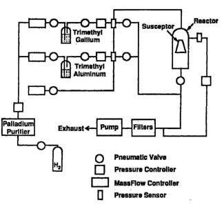
Precursors for the MOCVD process are alkyl, alicyclic and aryl compounds. The MOCVD process allows the deposit of most metals. In electronics the most interesting materials for deposition are carbides and nitrides. Composition of different materials require different working temperatures and pressure, different precursors and reactions.
These details can be provided at special catalogues and reference literature. The MOCVD process is usually used for growing the following heterostructures: HgCdTe detectors, GaAs/AlGaInP lasers, GaAs/InGaP HNTs, high power, orange LEDs, GaAs on Si wafers, InP/InGaAs quantum wells, solar cells, InP/InGaAsP lasers and some others.
The CVD processes combines processes like plasma CVD, lasers and photo CVD. They are different from the method when applying the required energy. That is the determining part of the CVD equipment. [2]
[1] “Chemical Vapor Deposition (CVD) worth $25.0 Billion and Physical Vapor Deposition (PVD) worth $24.3 Billion by 2019”, Markets and Markets Research Private Limited.
[2] “Handbook of Chemical Vapor Deposition. Principles, Technology and Application”, Hugh O.Pierson, 2nd ed.