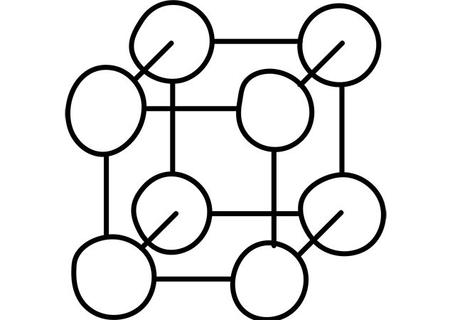
Semiconductors are a class of materials with electron conductivity. Their resistance value is between metal and insulator resistances at normal temperatures. The main feature of semiconductors is their ability to change features with different external conditions (temperature, light, electric and magnetic field and others).
Semiconductors have a negative resistance temperature coefficient. Semiconductor properties depend on the impurities in a crystal. Impurities in a semiconductor change conductance and temperature dependence. Impurities decrease a metal’s conductance, but does not change its temperature dependence.
Semiconductors – electrons and holes
Free electrons in semiconductors are caused by temperature and chemical purity of material. Semiconductors can be intrinsic and extrinsic, depending on their rate of purity.
An intrinsic semiconductor is a semiconductor where you can ignore the impurities. In intrinsic semiconductors the valence band is full at 0K – the conduction band is empty. Conduction and valence bands are divided by a forbidden band in a semiconductor. When the temperature is higher than zero, it is possible that some electrons will move to the conduction band, because of temperature fluctuations, creating some conductivity in a semiconductor. When an electron moves to the conduction band in an intrinsic semiconductor, holes are created in the valence band. Holes help electrons move to the higher free energy levels in the conduction band. Electron behaviour in the valence band can also be described as hole movement, the particles have positive charge, and some effective mass.
The higher temperature and smaller forbidden band, the bigger the rate of charge carriers (electron and hole) generation. At the same time as the generation of particles in the semiconductor, there are opposite processes in the semiconductor – a recombination of charge carriers when the electrons are getting back to the valence band, and the electron-hole pair disappears. There is always some concentration of electrons n0 and holes p0 in a semiconductor because of these two competing processes. In the intrinsic semiconductor, equilibrium concentration of electrons is equal to the equilibrium concentration of holes pi, and ni = pi.
Fremi-Dirac and Maxwell-Boltzmann statistics
All the states of electrons in the solid compounds can be described by Fermi-Dirac statistics.
According to this, every energy level can be occupied with electrons or holes. The sum of these two possibilities are:
The possibility to get the hole on the energy level is:
According to this distribution we can notice that energy of the hole is increasing when it moves down from Fermi level by energy scale. Usually the difference in energies of electrons and holes, and Fermi level, is quite significant for semiconductors. Ignoring 1 in the denominator of the energy distribution for holes, we will get the Maxwell-Boltzman statistics.
Electron gas
Electron gas for most semiconductors is non-degenerate. The possibility of occupation of energy levels by electrons and holes in a semiconductor is shown in Figure 8.
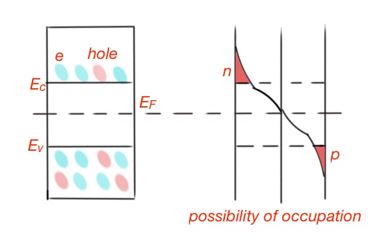
To estimate the concentration of electrons in semiconductors, we must resolve the following integral:
For holes the following applies:
An extrinsic semiconductor is a semiconductor where the electrical properties are considered by impurities. Impurities create additional energy levels in the forbidden band. If impurities concentration is small, the outer orbits do not interact, the distances between energy levels are large and levels are discrete. If impurity atoms are in the lattice sites – this is replacement impurity. If impurity atoms are in the interstitials – this is implementation impurity. Vacancies and interstitials can be impurities in a semiconductor lattice.
When impurity concentration is small, the possibility for an electron to make transitions between impurity levels are extremely small. The most frequent case are when impurities supply an electron to the conductance band, or accept from valence band, Figure 9.
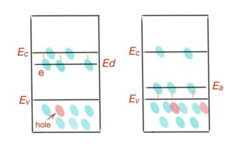
- Impurity energy levels are located in the forbidden band close to the bottom of the conductance band. Any small excitation can transfer electrons to the conductance band, where they can take part at the process of conductivity. Energy needed for this transition is much lower than the ionisation energy of an intrinsic semiconductor. Impurities, supplying electrons to the conductance band from their energy levels, are donors. Electron transition from the valence band directly to the conduction band occur very rarely. In these materials, electron concentration occur more often than hole concentration. That is why these semiconductors are called n-type semiconductors. The minimal energy needed to transfer electrons from the donor level to the conductance band is called donor energy ionisation.
- Impurity can bring free levels in a forbidden band, close to the top of the valence band. Due to the heating excitement, electrons transfer to the free levels of the forbidden band. Concentration holes in such a semiconductor is much bigger than the concentration of electrons. Electrons transferred into the conduction band do not take part at the conduction process. This semiconductor is p-type. Impurities, localising electrons from valence band into energy levels in a forbidden band are called acceptors. Minimal energy electrons should get to move to the acceptor level, which is called acceptor energy ionisation. Let’s consider an example:
Covalence semiconductors with replacement impurity
Suppose that in the Si crystalline lattice, some part of the atoms are replaced by atoms As. Inlining in the Si lattice, As atom gives four electrons for covalence bands creation – the fifth electron stays free. Orbit radius for this electron is around a couple of interatomic distances. And only small heating excitement is enough to take this electron out from an impurity atom. At the same time the impurity atom, that lost an electron, becomes a positively charged particle, fixed in a lattice. Replacement impurities, with valence bigger than valence of lattice atoms, are donors – Figure 10. Donor energy ionisation can be considered by the formula:
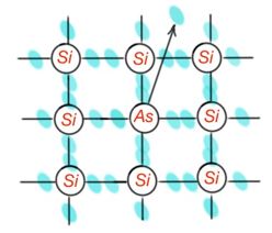
For Si , then energy ionization is 256 times less than hydrogen atom ionisation.
If the Si lattice inlined element has three electrons, it won’t be able to satisfy the fourth band with Si atom. Figure 11 shows the necessity to create four covalent bands, which can make an impurity atom get an electron from an Si atom, what will make an atom negatively ionized. Si atom will be positively ionised. In this case Si ion will have a localised hole. In this process of electron movement from atom to atom, the hole can move across the crystal. Replacement impurities with valence smaller than lattice atoms are called acceptors.
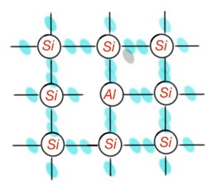
Basic and minor charge carriers
Charge carriers with bigger concentration in a given semiconductor is called basic charge carriers. When they have smaller concentration they are called minor charge carriers. For n-type semiconductors electrons are basic charge carriers, and holes are minor ones; for p-type semiconductors holes are basic charge carriers, electrons are minors.
When impurity concentration changes in a semiconductor, Fermi level also changes. The same applies for concentrations of holes and electrons. However, for intrinsic semiconductors at a given temperature in the thermodynamic equilibrium conditions, multiplication of both charge carrier concentrations is a constant value.
is an intrinsic concentration of charge carriers for semiconductors at a given temperature
Temperature ratio of charges concentration in semiconductors. Charge mobility in semiconductors
In the wide range of temperatures there is the following graph for concentrations of charge carriers for n-type semiconductors – Figure 12.
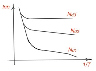 Figure 12. Concentration vs temperature for n-type semiconductor, where
Let us consider a curve for a small concentration of donors in a semiconductor. When the temperature is going up, the concentration of electrons are going up with the donor atom ionisation. Every donor can be considered as an atom located a hole. Then concentration of donors is equal to the hole concentration:
When the temperature is low, concentration of electrons is equal to the concentration of donors:
It means that the line slope characterises donor energy ionisation. During further temperature growth, all electrons appear in the conduction band, and their concentration is equal to the donor’s concentration. In some temperature ranges, electron concentration in a conduction band is constant – intrinsic conductance of a semiconductor is still not that large. This part of a temperature curve is called the depletion impurities region.
When the temperature is going up further, the dominant process in the conductivity becomes the excitement of intrinsic charge carriers. This temperature range is called the region of intrinsic conductivity. The temperature when this process starts is usually much higher than room temperature for most semiconductors. When impurity concentration increases, curves shift up. When impurities concentration increases, the distance between them on the energy scheme decreases, and their electron orbits interact stronger, and discrete energy levels split into impurity bands. The higher impurities concentration, the higher their depleting temperature.
When donor concentration is very high, like
, their ionisation energy is equal to zero, because the conduction band is overlapping into the impurity band. This semiconductor is called the degenerate semiconductor. Charge carrier concentration is constant for the n-type degenerate semiconductor in all the impurity conductivity ‘range’ – it can conduct current even at very low temperatures.
Fermi level
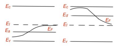
Fermi level characterises electron gas in a semiconductor. Let us find the position of Fermi level in a non-degenerate semiconductor:
When the temperature is very low, Fermi level is in the middle between the conduction and valence band in an n-type semiconductor. All n-type semiconductor behaviour patterns we considered works for p-type semiconductors as well. Figure 13 shows the Fermi level position depending on the temperature of a semiconductor for n-type and p-type semiconductors.
Charge carrier mobility
Charge carriers, under the influence of an external electric field, have directional speed and create an electric current. A charge carrier’s directional speed is called drift speed. Charge carrier mobility is a ratio of an average charge carrier drift speed to an electric field:
We have to differentiate electron mobility µn and hole mobility µp in semiconductors. Then current density in a semiconductor is the following:
n0 and p0 are equilibrium concentrations of electrons and holes in a semiconductor. Then semiconductor conductivity is:
For impurities, a semiconductor is one of the terms of this formula that can be ignored.
In accordance with experimental data, some semiconductors and insulators may have even better charge carrier mobility then metals.
Where l is a free path for charge carriers, u is a thermal speed for charge carriers.
Large charge carrier mobility can be the result of low effective mass m*, or large relaxation time τ0. Effective mass, in reality, can be bigger or smaller than electron mass. Relaxation time depends on the rate of electron dissipation in a crystal. Bigger electron collision frequency in a crystal, results in smaller relaxation time.
Electron average speed in a semiconductor and insulator for room temperature is about 105m/s, it corresponds to 70A wavelength. 5A is a wavelength for electrons in metals. It means point defects are irrelevant for electron dissipation in semiconductors and insulators.
The reasons of electrons dissipation in semiconductors can be lattice atoms or ions heating oscillations, impurities in ionised or normal state, and lattice defects. Cross-scattering of electrons can be ignored.
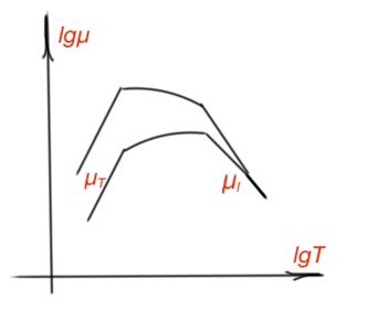
In the semiconductors with atomic lattice electrons, dissipation may happen on the lattice atoms or ions heating oscillations. These two dissipation mechanisms result in two parts of mobility temperature dependence. Let us consider µτ is a mobility, limited by electron dissipation on the heating oscillations of the lattice atoms. The free path will be the same for all charge carriers , and inversely proportional to temperature.
In the range of high temperatures, charge carrier dissipation on lattice atoms heating oscillations dominates, for low temperatures it is ionised impurities. Let us consider µl is a charge carrier mobility, limited by dissipation on the ionised impurities. Most of the impurities are in the ionised state because of small ionisation energy. Electrons are constantly facing attraction or repulsion from ions. And their free path will be ~u4. Concentration of ionised impurities Ni also plays an important role for electron dissipation.
And free path is inversely proportional to impurities concentration. Then:
The resulting mobility of charge carriers is the following:
Mobility temperature dependence can be seen in Figure 14.
Charge carrier interaction with an ion crystalline lattice is much stronger than with an atom crystalline lattice. Electron dissipation on the heating oscillations of the ions is very intensive, so electron mobility is very low for this kind of crystalline lattice. However, mobility estimations for an ion crystalline lattice are similar to the one for atomic lattice.
Conductance temperature dependence for semiconductors
For both atomic and ion crystalline lattices, when semiconductor temperature is increasing, charge carrier concentration increases exponentially. And this process plays a crucial role for conductance in a semiconductor. Figure 15 shows temperature dependence of semiconductor conductivity.
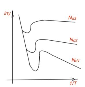
In the temperature range of impurities depletion, impurities concentration is constant, and electron mobility influences the semiconductor conductivity temperature rate. The decreasing conductivity in the low temperature is due to the charge carrier concentration decreasing (supplied by impurities), and charge carriers mobility decreasing (because of strong dissipation on ionised impurities). Conductance growth when temperature is increasing, corresponds to the intrinsic conductance of the semiconductor, when concentrations of electrons and holes are equal in a semiconductor. For this temperature region:
The curve in the region of intrinsic conductivity tells us the width of the forbidden band in a semiconductor.
For real semiconductor conductivity, temperature dependence can differ from the ones considered above. And there are several reasons for that. A semiconductor can contain not one, but two or more impurity atoms with different ionisation energies. Electrons and hole mobilities can be different, and that also influences conductance temperature dependence. If this difference is large, then intrinsic conductivity is not a minimal one. Then semiconductors may have minimal conductivity in the zone of mixed conductivity. In p-type semiconductors at low temperatures, electron conductivity can be ignored. When temperature is growing, hole concentration is the same, their mobility is decreasing, and concentration of electrons start to grow. At some temperature Ti point electron concentration will be valuable, and the semiconductor will be characterised by intrinsic conductivity. For this moment µnn0=µpp0. And minimal conductivity will be Υmin=2ep0µp. Then for a p-type semiconductor we get the following:
Non-equilibrium charge carriers and recombination mechanisms
At any temperature different from 0K, there are always some generation of electrons and holes in a semiconductor, due to heating excitation. Together with the charge carrier generation process, charge carrier recombination also occurs. Otherwise concentration of the charge carrier would grow, and the atoms in a lattice would ionise. Equilibrium is establishing between these two processes that corresponds to the equilibrium concentration of electrons and holes n0 and p0. In addition to thermal generation, other mechanisms of charge carrier generation are possible, like light irradiation of a semiconductor, or electromagnetic field application, and some others. As a result, some additional non-equilibrium concentration of charges occurs in a semiconductor. This non-equilibrium concentration can be described by the following equations:
Where and p and n are non-equilibrium concentrations. After the termination of non-thermal excitation, charge carrier concentration returns to its equilibrium values, by the process of recombination. And additional charge carrier concentration decreases to zero.
Generation process can be characterised by the rate of generation g – quantity of charge carrier pairs generating per unit of time in the unit of the semiconductor volume.
Recombination process can be described by the rate of recombination r – quantity of charge carrier pairs generating per unit of time in the unit of the semiconductor volume.
Cross-band or direct recombination happens when charge carriers are transiting from the conductivity band direct to the valence band on one the free energy levels. It corresponds to the disappearing of one pair electron – hole in a semiconductor. Figure 16a. However, this recombination process happens very rarely.
Trap recombination, Figure 16b and c. This is an example of non-direct recombination, that happens through energy levels, that are called traps. Recombination traps are impurities and defects that create energy levels in a forbidden band located at some distance from its boundaries. This recombination goes by two steps. If the trap level is free, then the first step is trapping of the electron from the conduction band. This electron leaves the process of current conductivity. The trap will keep an electron until the hole occurs close enough. Then the second step occurs – the electron moves on the free level in the valence band. If at the initial moment, the trap already contain an electron, then the first step is to transfer it on the free level in valence band, as soon as the hole is close enough. And second step is to accept an electron from conductance band. Traps are sensitive to the laws of momentum and energy conservation.
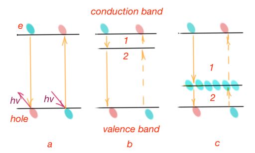
Any imperfections in the crystals can be a recombination of traps: impurity atoms or ions, vacancies, cracks, and another bulk or surface defects. The surface of a crystal contains many more defects. In addition to recombination traps, there are also traps, localising only one type of charge carrier. These traps interact with only one band – valence or conductance. After trapping a charge carrier, its releases the carrier after some time, and the charge carrier can take part in the conduction process. However, non-equilibrium charge carriers leave the process of recombination and these kind of traps can slow the process of recombination in a crystal.
The role of the same traps can change, depending on the external conditions – temperature or other influences.
Excessive energy, released during recombination of electrons and holes, can emit in a form of a photon, or transmit to the lattice in a non-radiant way (in the form of phonon). Interband radiant recombination is important for semiconductors with a narrow forbidden band at high temperatures (from room temperature and more). Semiconductors with a wide forbidden band are characterised with recombination through impurities. However, under some exact conditions, even these semiconductors can demonstrate interband radiant recombination. This process can be enhanced with very pure semiconductors, with a high concentration of electrons. For example, or – acts of radiation recombination in these semiconductors can exceed 80%.
Recombination of charge carriers is characterised by lifetime and diffusion path of non-equilibrium charge carriers. Recombination life time is a ratio of excessive concentration of charge carriers in a semiconductor, to the rate of change of this concentration due to recombination:
The most frequent case is when the concentration of charge carriers of one sign is constant. This case is typical for semiconductors with high pronounced impurity conductivity, after excitation of small excessive concentration of non-equilibrium charge carriers. Non-equilibrium charge carriers do not provoke significant change of basic charge carriers concentration. The recombination rate is proportional to the excessive concentration of non-basic charge carriers. Life time is constant. This type of recombination is called linear recombination.
Life time is a time when excessive concentration of charge e carriers will change times during linear recombination, or existence time of excessive concentration of charge carriers. Life time is determined by the quantity and type of recombination traps in a crystal, it is characterised by the chemical purity of a semiconductor. Life time is maximum in the semiconductor with intrinsic conductivity. For real semiconductors life time of non-equilibrium charge carriers is in the range 10-2 – 10-10 sec.
If generation of non-equilibrium charge carriers occur only in some part of a semiconductor, then the local area forms with excessive concentration of charge carriers. It causes diffusion current in a semiconductor. Diffusion current may occur without an electromagnetic field, and is due to charge carrier gradient in a semiconductor. Non-equilibrium charge carriers are recombining during diffusion. That is why diffusion current is fading.
Diffusion path is the distance in semiconductor where excessive concentration of charge carriers is decreasing time, in the absence of an electromagnetic field.
Where Dn and Dp are diffusion coefficients for electrons and holes. Less defects and impurities in a semiconductor, bigger diffusion path and life time of non-equilibrium charge carriers.
#9: Optical and photoelectrical properties of semiconductors

