Objective:
The purpose of this activity is to investigate the forward and reverse current vs. voltage characteristics of an MOS field effect transistor (NMOS and PMOS) connected as a diode.
Materials
- ADALM2000 active learning module
- Solderless breadboard
- One 100Ω resistor
- One ZVN2110A NMOS transistor
- One ZVP2110A PMOS transistor
NMOS directions
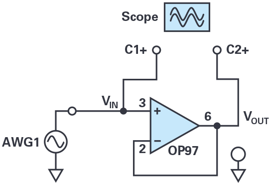
The current vs. voltage characteristics of the gate source of an enhancement mode NMOS transistor can be measured using the ADALM2000 lab hardware and the following connections. Set up the breadboard with the waveform generator, W1, attached to one end of resistor R1. Connect Scope Input 2+ here as well. Connect the gate and drain of M1 to the opposite end of R1 as shown in the diagram. The source of M1 is connected to the negative power supply Vn (–5V). Connect Scope Input 2– and Scope Input 1+ to the gate-drain node of M1. Scope Input 1– is best grounded to reduce noise pickup. Be sure that the power supply, Vn, is turned off while you build your circuit. Once you are sure that all of your connections are correct, turn on the supply.
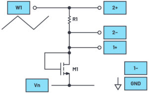
Figure 1. NMOS diode connection diagram
Hardware setup
The waveform generator should be configured for a 100Hz triangle wave with a 10V amplitude peak-to-peak and 0V offset. Differential Scope Channel 2 (2+, 2–) measures the current in the resistor (and in the transistor). The single-ended input of Scope Channel 1 (1+) is connected to measure the voltage across the transistor. The current flowing through the transistor is the voltage difference 2+ and 2– divided by the resistor value (100Ω).
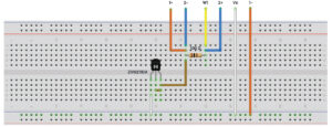
Figure 2. NMOS diode breadboard circuit
Procedure
Load the captured data into Excel and calculate the current. Calculate and plot the current vs. the voltage across the transistor (VGS). No current should flow in the reverse direction. In the forward conduction region, the voltage-current relationship should be quadratic. Calculate and plot the square root of the current vs. VGS. Compare the shape of the two plots and comment.
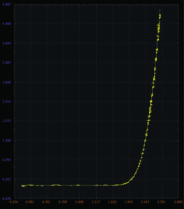
Figure 3. NMOS diode XY plot
PMOS directions
Repeat the experiment using the PMOS device. The connections are similar, as shown in Figure 4. You may notice that the polarity of the scope inputs has been reversed in this case. This is so that the direction of the voltage and currents on the scope screen will be similar to the NMOS case. The source of M1 is connected to the positive power supply Vp (+5V). Connect Scope Input 2+ and Scope Input 1– to the gate-drain node of M1. Be sure that the power supply (Vp) is turned off while you build your circuit. Once you are sure that all of your connections are correct, turn on the supplies.
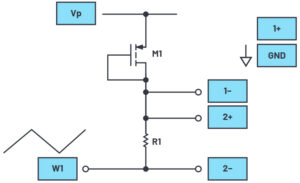
Figure 4. PMOS diode connection diagram
Hardware setup
The waveform generator should be configured for a 100Hz triangle wave with a 10V amplitude peak-to-peak and 0V offset. The differential scope channel 2 (2+, 2–) measures the current in the resistor (and in the transistor). The single-ended input of Scope Channel 1 (1–) is connected to measure the voltage across the transistor. The current flowing through the transistor is the voltage difference 2+ and 2– divided by the resistor value (100Ω).
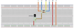
Figure 5. PMOS diode breadboard circuit
Procedure
Load the captured data into Excel and calculate the current. Calculate and plot the current vs. VGS. No current should flow in the reverse direction. In the forward conduction region, the voltage, current relationship should be quadratic. Calculate and plot the square root of the current (ID) vs. VGS. Compare the shape of the two plots and comment.
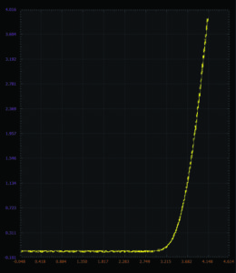
Figure 6. PMOS diode XY plot
Questions
By plotting the data measured for ID vs. VGS, find and report values of VTH and K (W/L). How do the VTH and K (W/L) values for the NMOS and PMOS compare? You can find the answer at the StudentZone blog.
By Doug Mercer, Consulting Fellow, and Antoniu Miclaus, System Applications Engineer, Analog Devices.