Next-generation devices made with new “peel and stack” method may include electronic chips worn on the skin.
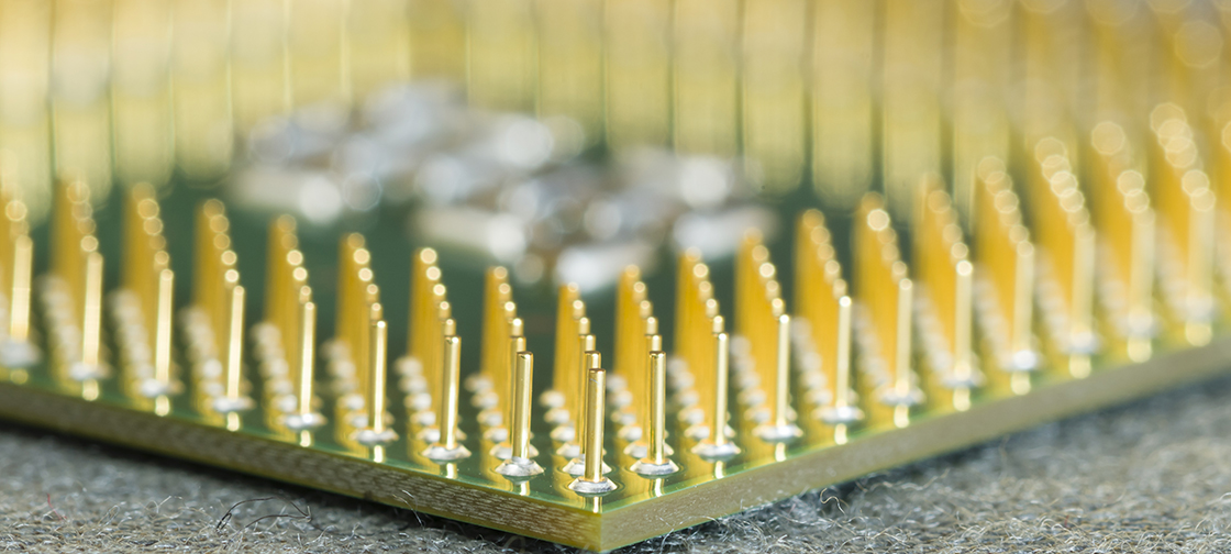
At the heart of any electronic device is a cold, hard computer chip, covered in a miniature city of transistors and other semiconducting elements. Because computer chips are rigid, the electronic devices that they power, such as our smartphones, laptops, watches, and televisions, are similarly inflexible.
Now a process developed by MIT engineers may be the key to manufacturing flexible electronics with multiple functionalities in a cost-effective way.
The process is called “remote epitaxy” and involves growing thin films of semiconducting material on a large, thick wafer of the same material, which is covered in an intermediate layer of graphene. Once the researchers grow a semiconducting film, they can peel it away from the graphene-covered wafer and then reuse the wafer, which itself can be expensive depending on the type of material it’s made from. In this way, the team can copy and peel away any number of thin, flexible semiconducting films, using the same underlying wafer.
In a paper published today in the journal Nature, the researchers demonstrate that they can use remote epitaxy to produce freestanding films of any functional material. More importantly, they can stack films made from these different materials, to produce flexible, multifunctional electronic devices.
The researchers expect that the process could be used to produce stretchy electronic films for a wide variety of uses, including virtual reality-enabled contact lenses, solar-powered skins that mold to the contours of your car, electronic fabrics that respond to the weather, and other flexible electronics that seemed until now to be the stuff of Marvel movies.
Source: “New technique for new stretchy electronics”, Jennifer Chu, MIT News Office