After the introduction of the SMU ADALM1000 it is good to continue with the seventh part of our series with some small, basic measurements.
By Doug Mercer and Antoniu Miclaus, Analog Devices
Objective: The objective of this lab activity is to study the phenomenon of resonance in RLC circuits. Determine the resonant frequency and bandwidth of the given network using the amplitude response to a sinusoidal source.
Background: A resonant circuit, also called a tuned circuit, consists of an inductor and a capacitor together with a voltage or current source. It is one of the most important circuits used in electronics. For example, a resonant circuit, in one of many forms, allows us to tune into a desired radio or television station from the vast number of signals that are around us at any time.
A network is in resonance when the voltage and current at the network input terminals are in phase and the input impedance of the network is purely resistive.
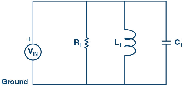
Consider the parallel RLC circuit of Figure 2. The steady-state admittance offered by the circuit is .
Resonance occurs when the voltage and current at the input terminals are in phase. This corresponds to a purely real admittance, so that the necessary condition is given by .
The resonant condition may be achieved by adjusting L, C, or ω. Keeping L and C constant, the resonant frequency ωo is given by .
Or .
Frequency response is a plot of the magnitude of the output voltage of a resonance circuit as a function of frequency. The response of course starts at zero, reaches a maximum value in the vicinity of the natural resonant frequency, and then drops again to zero as ω becomes infinite. The frequency response is shown in Figure 3.
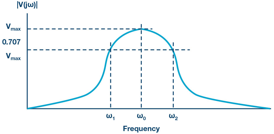
The two additional frequencies ω1 and ω2 are also indicated; these are called half-power frequencies. These frequencies locate those points on the curve at which the voltage response is 1/√2, or 0.707 times the maximum value. They are used to measure the bandwidth of the response curve. This is called the half-power bandwidth of the resonant circuit and is defined as .
Materials:
- ADALM1000 hardware module
- Resistors: 100 Ω, 1 kΩ
- Capacitors: 1 µF, 0.01 µF
- Inductors: 20 mH
Procedure:
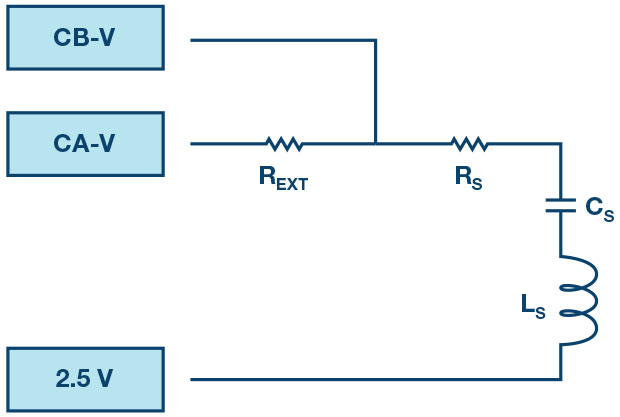
1. Set up the RLC circuit as shown in Figure 5 on your solderless breadboard, with the component values RS = 100 Ω, R1 = 1 kΩ, C1 = 1 µF, and L1 = 20 mH.
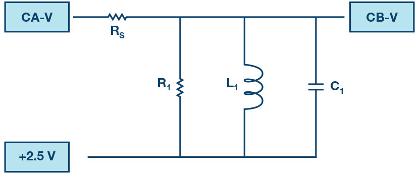
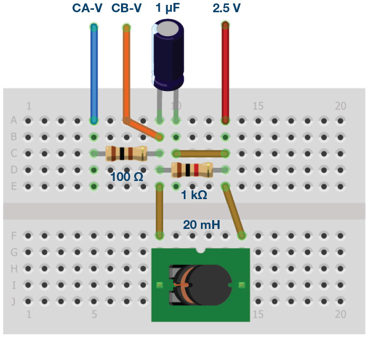
2. Set the Channel A AWG Min value to 0.5 and AWG Max value to 4.5 V to apply a 4 V p-p sine wave centered on 2.5 V as the input voltage to the circuit. From the AWG A Mode drop-down menu, select SVMI mode. From the AWG A Shape drop-down menu, select Sine. From the AWG B Mode drop-down menu, select Hi-Z mode.
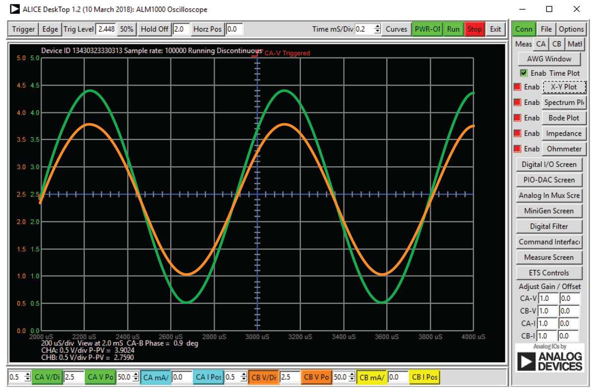
3. From the ALICE Curves drop-down menu, select CA-V and CB-V for display. From the Trigger drop-down menu, select CA-V and Auto Level. Set the Hold Off to 2 ms. Adjust the time base until you have approximately two cycles of the sine wave on the display grid. From the Meas CA drop-down menu, select P-P under CA-V and do the same for CB. Also from the Meas CA menu, select A-B Phase.
4. Vary the frequency of the sine wave on the AWG A menu from 500 Hz to 2.5 kHz in 100 Hz steps. For each frequency, write down the p-p voltage for Channel A and Channel B and the A-B phase. Note the frequency where the voltage is maximum at the output of the circuit for Channel B. This will be near the resonant frequency of the circuit. Note that the phase should be nearly 0° at this frequency. Adjust the frequency in 10 Hz increments around where you see a maximum for CB p-p voltage until the A-B phase is exactly zero.
5. Repeat the experiment using for the series resonant circuitry in Figure 4, and use L1 = 20 mH and C1 = 0.01 μF, and R1 = 1 kΩ. The Vo voltage on the resistor is proportional to the series RLC circuit current.
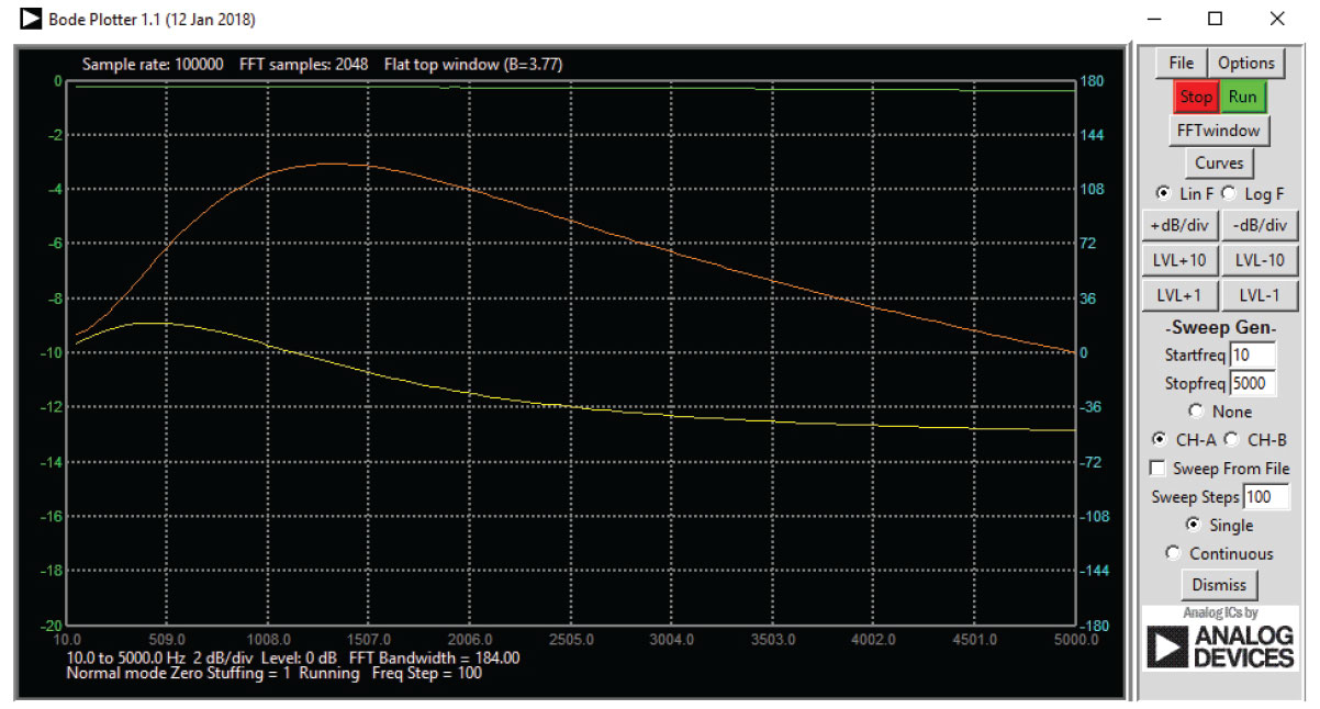
Frequency Response Plots with the ALICE-Bode Plotter
The ALICE-Bode Plotter software can make generating frequency and phase response plots much easier. Using the parallel resonate RLC circuit in Figure 5, we can sweep the input frequency from 10 Hz to 5000 Hz and plot the signal amplitude of both Channel A and Channel B and the relative phase angle between Channel B and Channel A.
- With the circuit connected to the ALM1000, as in Figure 5, start the ALICE-Bode Plotter from the ALICE main interface.
- Under the Curves drop-down menu, select CA-dBV, CB-dBV, and Phase B-A.
- Select Lin F for a linear representation of the sweep.
- Under the Options drop-down menu, click on Cut-DC.
- Set the AWG Channel A Min value to 1.086 and Max value to 3.914. This will be a 1 V rms (0 dBV) amplitude centered on the 2.5 V middle of the analog input range. Set AWG A mode to SVMI and Shape to Sine. Set the AWG Channel B to Hi-Z Mode. Be sure the Sync AWG check box is selected.
- Under the Sweep Gen menu, use Startfreq to set the frequency sweep to start at 10 Hz and use Stopfreq to set the sweep to stop at 5000 Hz. Select CH-A as the channel to sweep. Also use Sweep Steps to enter the number of frequency steps, which should be set to 100.
- You should now be able to press the green Run button and run the frequency sweep. After the sweep is completed, you should see something like the screenshot in Figure 8. You may want to use the LVL and dB/div buttons to optimize the plots to best fit the screen grid.
Questions:
1. Find the resonant frequency, ωo using Equation 1 and compare it to the experimental value in both cases.
2. Plot the voltage response of the circuit and obtain the bandwidth from the half-power frequencies using Equation 3.
Appendix:
Notes
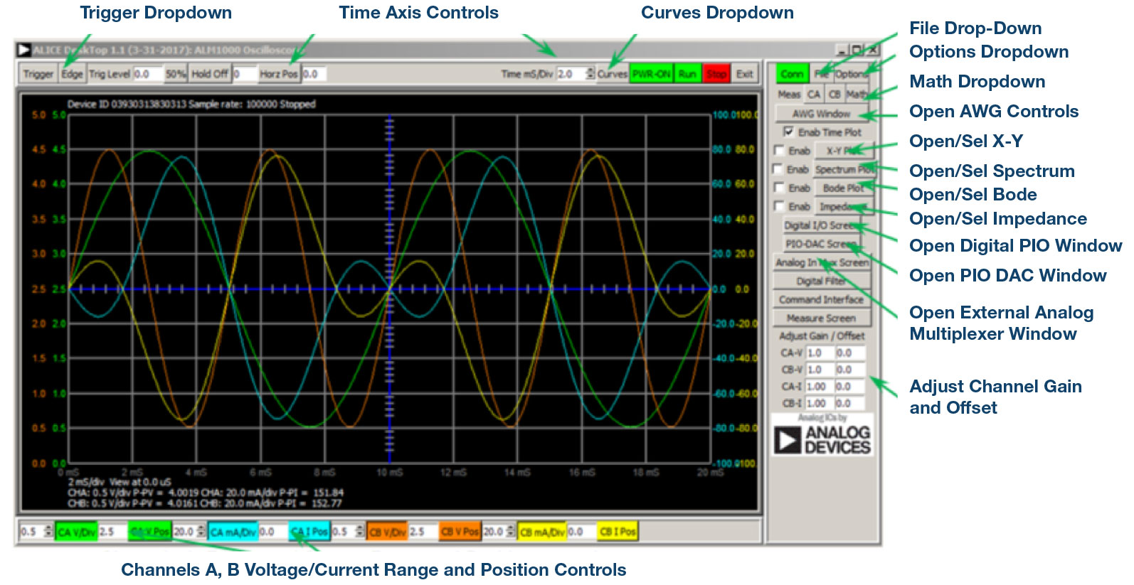
As in all the ALM labs, we use the following terminology when referring to the connections to the ALM1000 connector and configuring the hardware. The green shaded rectangles indicate connections to the ADALM1000 analog I/O connector. The analog I/O channel pins are referred to as CA and CB. When configured to force voltage/measure current, –V is added (as in CA-V) or when configured to force current/measure voltage, –I is added (as in CA-I). When a channel is configured in the high impedance mode to only measure voltage, –H is added (as in CA-H).
Scope traces are similarly referred to by channel and voltage/current, such as CA-V and CB-V for the voltage waveforms, and CA-I and CB-I for the current waveforms.
We are using the ALICE Rev 1.1 software for those examples here. File: alice-desktop-1.1-setup.zip. Please download here.
The ALICE Desktop software provides the following functions:
- A 2-channel oscilloscope for time domain display and analysis of voltage and current waveforms.
- The 2-channel arbitrary waveform generator (AWG) controls.
- The X and Y display for plotting captured voltage and current vs. voltage and current data, as well as voltage waveform histograms.
- The 2-channel spectrum analyzer for frequency domain display and analysis of voltage waveforms.
- The Bode plotter and network analyzer with built-in sweep generator.
- An impedance analyzer for analyzing complex RLC networks and as an RLC meter and vector voltmeter.
- A dc ohmmeter measures unknown resistance with respect to known external resistor or known internal 50 Ω.
- Board self-calibration using the AD584 precision 2.5 V reference from the ADALP2000 analog parts kit.
- ALICE M1K voltmeter.
- ALICE M1K meter source.
- ALICE M1K desktop tool.
For more information, please look here.
Note: You need to have the ADALM1000 connected to your PC to use the software.
Doug Mercer [doug.mercer@analog.com] received his B.S.E.E. degree from Rensselaer Polytechnic Institute (RPI) in 1977. Since joining Analog Devices in 1977, he has contributed directly or indirectly to more than 30 data converter products, and he holds 13 patents. He was appointed to the position of ADI Fellow in 1995. In 2009, he transitioned from full-time work and has continued consulting at ADI as a Fellow Emeritus contributing to the Active Learning Program. In 2016 he was named Engineer in Residence within the ECSE department at RPI.
Antoniu Miclaus [antoniu.miclaus@analog.com] is a system applications engineer at Analog Devices, where he works on ADI academic programs, as well as embedded software for Circuits from the Lab® and QA process management. He started working at Analog Devices in February 2017 in Cluj-Napoca, Romania. He is currently an M.Sc. student in the software engineering master’s program at Babes-Bolyai University and he has a B.Eng. in electronics and telecommunications from Technical University of Cluj-Napoca.