Nanotechnology is a technology in the nanoscale. Nanotechnology can be applied to different fields like physics, chemistry, biology and particularly nanoelectronics. Nanoelectronics deals with individual atoms or molecules to the structures of submicron size.
Nanoscale objects are a build up of their elemental constituents. These elemental constituents can be assembled into a nanostructure due to syntheses, self-assembly, solution with reagents, and chemical growth. Nanostructures size ranges from 1 to 102nm, the molecules or atoms can aggregate to the structure consisting of 10-105 pieces.
Different kinds of vacuum depositions and plasma techniques create nanostructures (including nanoelectronics). The techniques like molecular-beam epitaxy and vapour-phase epitaxy are used for production of atomically controlled nanostructures for nanoelectronics. Also top-down litographic and non-litographic techniques are used to create nanoscale devices.
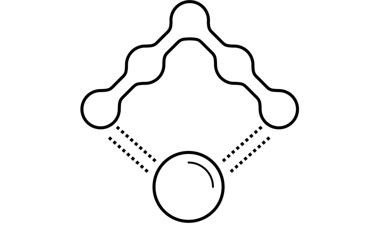
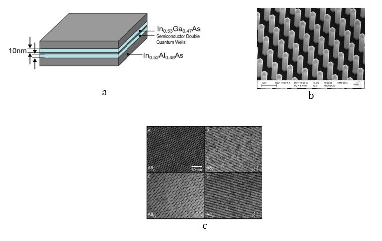
We will discuss the methods of the creation of nanoelectronic devices below and over this course. We will also cover methods of their investigation. Creation of nanodevices demand a special approach for experimental and computational tools. The properties of materials at a nanoscale are very different from the properties of the same large scale materials. If the three-dimentional structure is characterised by one-dimension, that being nanoscale, then this structure is called a quantum well. If two dimensions are nanoscale, the structure is known as nanowire. If three-dimensions are nanoscale, the structure is a quantum dot. Figure 1 depicts an example of nanostructures (quantum wells, wires and dots).
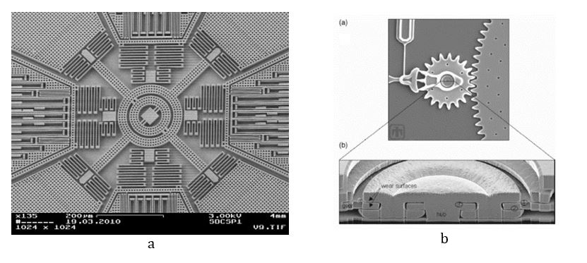
One of the most used micro/nanoelectro devices are MEMS/NEMS. Figure 2 shows a picture of MEMS and NEMS. MEMS sizes are less then 1mm, and they combine microactuators, microsensors and other microstructures. Technological developments go forward to develop micro- and nanostructural electronic devices.
Many micro/nanoscale devices are produced for different applications like industrial, consumer and others. The most popular usage of MEMS is accelerometers in smartphones and wearable devices, and also variable kinds of pressure sensors.
NEMS are nearly identical to MEMS, but they are much smaller. The developers use an bottom-up, up-bottom approach to build NEMS devices, and sometimes a combination of these two techniques. The top-bottom approach is a technique based on a slicing or cutting of the bulk of materials in order to get the nano-scale device. The bottom-top approach is based on the self-assembly of atoms or molecules. NEMS include cantilevers for microscopes like scanning tunnelling microscopy, atomic force microscopy and other nanostructures. Nanoelectronics can be used to produce molecular switches, transistors, nanotube flat-panel displays, nanotube integrated circuits, nanoscopic lasers and others.
#2.1 MEMS technology and devices - classification and a concept