This post answers the question “How does molecular beam epitaxy work?”. Molecular beam epitaxy (MBE) is the technique of semiconductor material growth – a form of vacuum evaporation with material quality control along the process. Molecular beam epitaxy usually occurs in an ultra-high vacuum environment with pressures of Torr with the impurity gases.
Molecular beams are the formation of components on the heterostructure deposit, chemically reacting to each other on the heated structure. The MBE process allows us to obtain a very precise structure from the point of view of constituent materials. The utilisation of the solid-state sources allows us to create a high quality heterostructure.
There are a few forms of epitaxy that exist – III-V group source epitaxy is called GSMBE, V-group source epitaxy is called MOMBE, and so chemical beam epitaxy combines MOMBE and GSMBE techniques.
The basic part of the equipment for the MBE process is called the MBE growth reactor, where the growth process occurs. The important parts of the MBE equipment are the effusion cells, containing the operating gases; the rotating substrate handle; wafer manipulation; shatters (artificially stopping the growing fluxes) and some others.
A simplified structure of the MBE system, that shows how does molecular beam epitaxy work, is depicted in Figure 1.
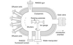 Figure 1. The schematic structure of the MBE process equipment.
The growth process occurs when growing materials from non-interacting beams of atomic and molecular sources deposit on the heated surface of the substrate, combining into the thin film with variable parameters. Variable parameters of the film like growth rate, doping concentration, and others depend on the constituent parts of the materials of the MBE process. The ultra-high vacuum of the environment of the MBE process allows us to manufacture high purity films with very precise characteristics and materials. [1] [1] “Thin films and epitaxy: basic techniques, and materials, processes and technology. Handbook of crystal growth”, chapter 4, Elsevier, 2015
More educational content can be found at Reddit community r/ElectronicsEasy.