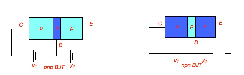
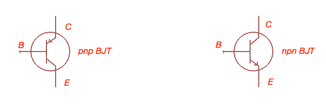
BJT transistor is a three terminal semiconductor device, based on three layers of p and n layers, with different doping concentration. BJT transistor can be two types – pnp and npn BJT transistor.
Bipolar junction transistor (BJT) is characterised by three regions – base (B), collector (C) and emittor (E). Base and collector layers are lightly doped, emitter layer – is heavily doped.
Charges flow at the BJT are depicted on the figure below.
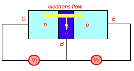
Let’s consider pnp transistor. It is consist of two pn junctions. One junction is forward-biased, and the other is reverse-biased. Majority of careers are moving from E across forward-biased pn-junction. B layer is usually thin, but characterised with high resistivity, so majority of careers will flow through into the C layer (due to different doping levels of these materials).
Currents in BJT transistor can be found with Kirchhoff’s Law: .
Note that collector current will consist of leakage current and majority careers current .
In the DC mode emitter and collector currents will be related with the ratio . For the AC mode ratio is more complex and different for vaious values of currents .
For DC circuit there is s ratio, that shows relation between base and collector currents across the circuit , is a common emitter amplification factor. In case of AC circuit this parameter will vary in accordance to formula .
These two amplification factors are related by the formula . Another relationship for BJT currents we can derive is .
The main feature of BJT – small base-collector current controlling large collector current.
Common-emitter configuration
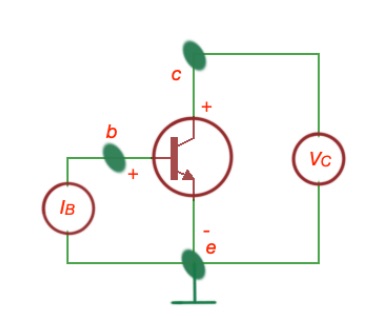
This configuration is called common-emitter as emitter is common for input and output voltages. PNP BJT common emitter configuration is depicted on the figure below.
Currents in the circuit are related with the ratios: , .
Here collector-base junction is reverse biased, and base-emitter junction is forward-biased. Input data will be here base-emitter, and output – collector-emitter.
In the active region here base-collector pn-junction is reverse-biased and base-emitter pn-junction is forward-biased.
Common – base configuration
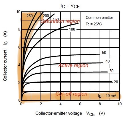
This configuration is called that, because base is connected to both – emitter and collector. The output characteristics of BJT can be divided into three areas – cut-off, saturation and active region.
In the cut-off region both collector-base and emitter-base pn-junctions are reverse-biased – transistor is off.
In the active region , base-collector pn-junction is reverse-biased, and base-emitter – forward-biased.
Let’s imagine ideal voltage source, injecting current through base region, junction base-emitter becomes forward-biased. Varying the current from ideal voltage source, you can manage current . If this ideal voltage source is connected to the collector circuit, current also can be controlled. The circuit for determination of BJT I-V curve is depicted on the figure below.
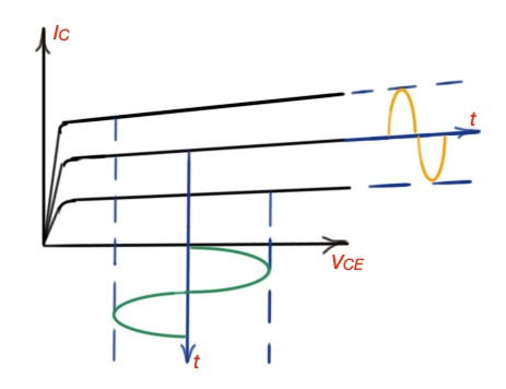
The most important dynamic characteristics of a BJT are it’s switching characteristics. In standard operation the BJT transistor works as an amplifier.
Let’s apply to the base AC signal and DC signal and we will see the amplification on the resulting curve, so all oscillations of the base current is resulting in amplified collector current.
Important point to consider is self-biased BJT circuit, that is depicted below. It can be transformed into circuits that are much easier to consider from the point of view of BJT operation point.
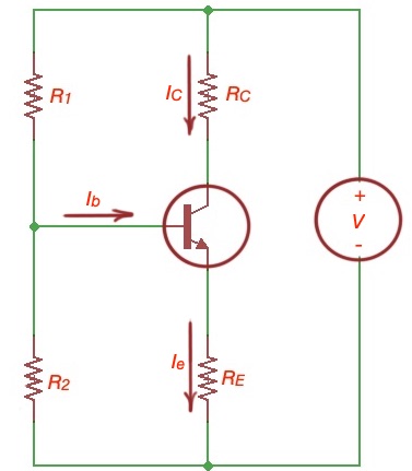
Using Thenevin theorem we can transform the circuit into the following circuit below with equivalent resistance and voltage source.
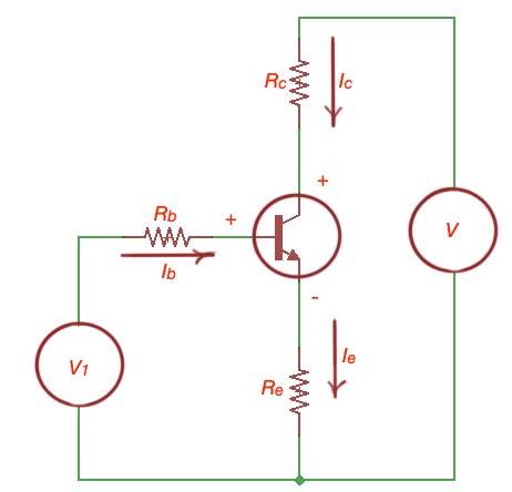
Here equivalent voltage source is , and is an equivalent base resistance. Here .
, then . , . .Then and .
The BJT becomes a switch as soon as the base is sourced by the AC signal, so it will work in the conducting regime to the blocking regime. The dynamic switching characteristics here are also very important, because the high-frequency velocity makes a huge impact on the losses of the device.
On figure below we can see the volt-ampere characteristics for the npn BJT. To drive it as an amplifier the transistor must be kept in its linear region. For using the transistor as a switch, it should operate from the cut-off region to the saturation region – turning on and turning off.
The turn-on region is characterised by the increase in the collector current, when the collector-emitter voltage remains small. The depletion region in the transistor becomes very small and as conductivity increases, it corresponds to the saturation region in Figure 1.
The turn-off region is characterised with a high collector-emitter voltage and low collector current level, which corresponds to the cut-off region. So switching losses occur when the device switches in high frequency. The rising and falling times of the signal plays very important role.
In order to calculate the power losses for the transistor it is helpful to use the formula , here and are the maximum values of voltage and current, and are the switching time and frequency.