Besides the resistive function, MOSFETs can also perform an amplification function. Let’s consider how we can obtain the amplification function from a MOSFET.
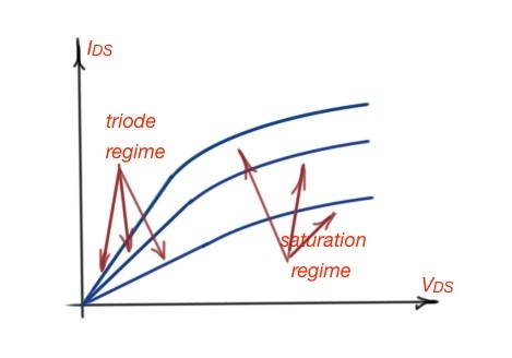
Figure 1. The transverse characteristic of MOSFET operation. There are three lines depicted that are the focus of the .
Figure 1 depicts the transverse characteristics for a MOSFET. During the MOSFET operation we can see three working regimes – the triode regime, off-regime and saturation regime. During the off-regime, the MOSFET does not operates.
The triode regime characterises the resistive operation of a MOSFET. The saturation regime characterises the amplification function of the MOSFET. As we know corresponds to the triode regime, the saturation regime is . In the saturation regime the MOSFET works as a current source. The operation of a MOSFET can be represented as the switch current source (SCS) model, which is used only at the saturation operation model. The SCS model of the MOSFET is depicted in Figure 2.
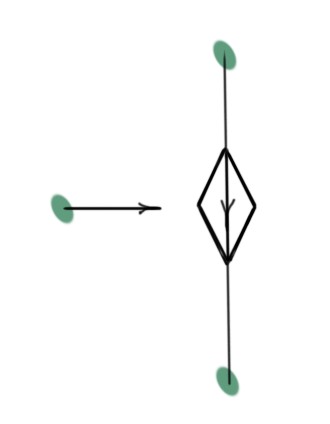
Figure 2. The SCS model of a MOSFET amplifier.
When the MOSFET is in the saturation regime, it will be characterised with the following parameters: , and the saturation regime works only when , so the .
Modern amplifiers are usually manufactured using the MOSFET’s inside. Let’s consider the simplified scheme of the amplifier, depicted in Figure 3. Let’s find the output voltage as the function of input voltage .
In accordance to the circuit . The ratio of . This relationship is a transfer function of the amplifier, and is depicted in Figure 4. This ratio shows the voltage gain of the amplifier, and it is a non-linear function and depends on the input voltage, that positions the MOSFET in the saturation regime.
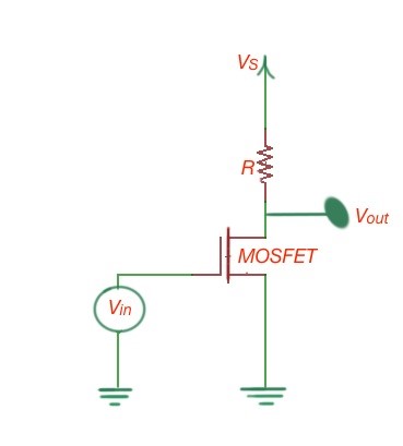
Figure 3. Simplified scheme of the MOSFET.
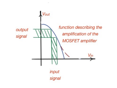
Figure 4.The input vs output voltage ratio for the MOSFET amplifier.
In practical amplifiers, the input and output are tied up to the same ground. In order for every input signal to be amplified, it should match a certain range of voltages, so we can use bias voltages for these purposes.
Let’s consider the input voltage as the sum of the input voltage, plus the biased voltage . The output voltage in this case will consist of two constituents . As far as is the amplified voltage of , the is the amplified voltage of . The bias voltage is important as it affects the operation point, so the operation point for the amplifier is called the amplifier bias point.
A large signal model of the MOSFET amplifier helps to answer the question of the relationship between the output voltage and input voltage, when the input voltage changes significantly, and what is the valid voltage range for a MOSFET amplifier? The valid voltage range for the MOSFET amplifier is the band of input voltages when the MOSFET amplifier works in the saturation regime. The lowest valid input voltage is , the highest is .