Memory is a very important part of a computer that stores programs and data. It can be classified as non-volatile and volatile. First of all it stores the content, and second it erases the content when the power is on. Non-volatile memory is very important as it stores the boot code for the computer so it can start work when powered.
Volatile memory stores dynamic variables when a computer is operating, and it can consist of two parts:
• Dynamic, when memory contents can be erased and written again while the computer is powered;
• Static, memory that contains non-erasable pieces of data.
Non-volatile memory is designed as two parts – a part that does not expect to be rewritten during memory product lifetime, and a part that can be rewritten a number of times.
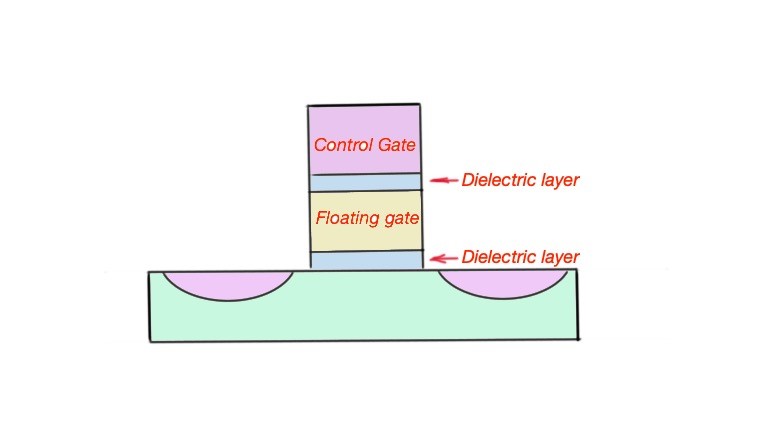
EEPROM (Electrically erasable and programmable read-only memory). This is a type of non-volatile memory. An EEPROM cell consists of one to two transistor structure devices. The voltage is supplied to the control gate. Depending on the threshold voltage level it may drive the current. The sensing amplifier transforms this to «1» or «0». The EEPROM physical structure is depicted on Figure 1.
Figure 1. General structure of the memory transistor.
EEPROM is usually stored in transparent package, as UV light plays an important role in controlling the work of the memory. EEPROM uses a synchronous interface which makes it easy to use.
There is two types of EEPROM:
• Parallel – this is expensive, has high density(>265kbit), and is used in special applications;
• Series – relatively non-expensive, has low density (<265kbit), and is used as a commodity product;
EEPOM is an expensive type of memory, allowing you to write/erase random units of data. This type of memory has a small size of available memory space and a physically small size. EEPROM is a good type of non-volatile small-sized memory.
Flash memory is similar to the EPROM memory. The advantage of flash memory is it is electrically driven, which means it is quicker to erase and write data. Flash memory is used in variety of products of consumer electronics, cars and many other applications, due to the flexibility of its usage.
Despite the fact that these two memory types are similarly structured, Flash memory has a very thin layer between the silicon substrate and the floating gate. So the active mechanism here is tunnelling. Flash memory is slightly more expensive than other memory types.
The designer can apply a range of voltages to the source and controlling gates. Flash memory operates by application of voltage to the controlling gate. Flash memory usually contains an internal voltage generator to support high controlling voltages.
Flash devices have the capacity of one million erase cycles. The modern flash memory designed to control the memory does not reach its erase limit during the device lifetime.
Flash memory is made of two types:
• NAND Flash memory;
• NOR Flash memory.
NOR Flash memory is a RAM type memory with direct access to the microprocessor for read/write operations, and has very good response time. NAND memory is a sequential access memory. It is well suited for storing large amounts of data, has very high density, low response time and high complexity.
Flash memory is structured by blocks, which improves the erasing process. So only desired blocks of information are erased. Flash memory of different manufacturers can differ from each other with pin assessments, programming algorithms and memory structure.
Flash memory can be different depending on the division blocks.
• Uniform-block memory is divided into equally sized blocks;
• Non-uniform-block memory or boot-block, which is often used to store the boot code of the microprocessor and other data. The memory blocks that store boot code are usually smaller and rarely accessed.
Data blocks of flash memory usually contain the hardware protection scheme, when the read/write operations are disabled for some data blocks, and can be enabled with exact voltage levels.
Flash memory reads faster than writes. The controlling logic of flash targets proper data blocks for erase or program mode, depending on the microprocessor orders. The operations that can be scheduled for data blocks can unlock cycles, command setup, erase/ write operation, device setup and identification process. The last process is needed for the microprocessor to check what part of the hardware is protected and what flash device is connected to the microprocessor.
Protection functions allows for the software to recognise what block of data is available for programming operations. Hardware protection is guaranteed by the higher enabling voltages and access pins, and then the normal operating process.
Static RAM (SRAM) is volatile memory, and exists in any computing device. It consists of the controlling and decoding logic in parallel to latches. Schematically an SRAM cell is depicted in Figure 2. The latch is structured with a set of transistors, and are combined with the looped inverters and two pass transistors.
Figure 2. SRAM feedback latch.
Dynamic RAM (DRAM) is a more cost effective type of RAM, where transistors and invertors are replaced with the capacitor as shown in Figure 3. DRAM architecture is depicted in Figure 4. It is structured as a matrix of bits with rows and columns, which determines the data adress. Rows and columns are multi–plexed onto the same pins. Row addresses are loaded and stored in the RAS (raw adress stobe). Column addresses are loaded and stored in the CAS (colums address strobe).
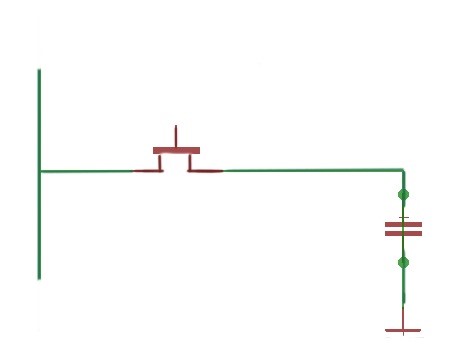
Figure 3. DRAM feedback latch.
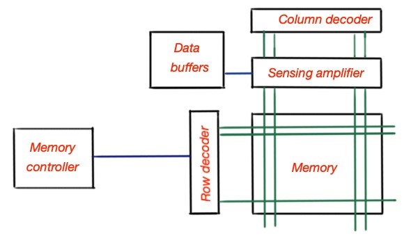
Figure 4. DRAM architecture scheme.
The DRAM chip should contain a sensitive amplifier, that detects capacitor charging times and maintains refresh operation of the DRAM. The whole data row is refreshed at the same time to maintain data integrity. DRAM modification with better performance is SDRAM (synchronous DRAM), where the synchronous bus interface accelerates data transaction.
The SDRAM process works as depicted in Figure 5. This operation is called the read-modify-write data process – when a piece of data is extracted from the memory, modified and placed back. This process significantly increases efficiency of this memory type.
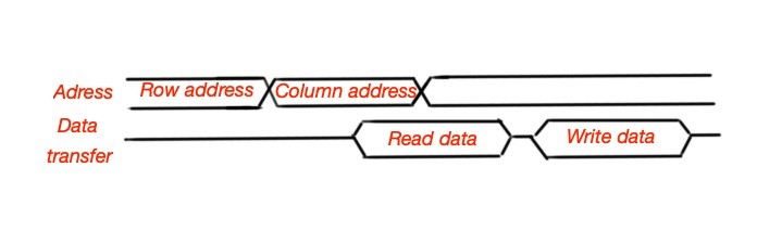
Figure 5. Read-modify-write transaction.
The fast page mode (FPM) DRAM memory type brings even more efficiency, and are used in CPUs.