The basic idea of a digital concept is discretion. The idea is to cut single values of a signal corresponding to the discrete-times of the chosen interval. Figure 1 depicts continuous and discrete signals. While the discretion or digital approach looks useless in the dynamic continuous range of variables, we will see that it has a big advantage compared to analogous or continuous signals from the point of view of noise.
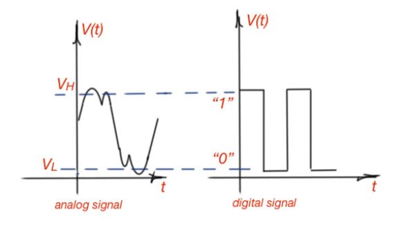
In the example above the digital signal only has two levels of precision – 0 or 1. Meanwhile analogous signals are characterised by countless levels of precision. Two levels of precision can be used in many applications. And the levels can also be TRUE or FALSE.
For some applications more levels of precision are more favourable. One of the most important approaches consists of coding multi-digital systems with bits, or binary digits. This approach helps to interpret multi-digit data to binary data. Binary data can be allocated by multiple wires, when each wire carries a bit, or multiple bits can be time multiplexed and carried by single wire.
The binary representation is a two-level representation. All digital circuits are based on the binary representation, because it is much easier to build a system based on the two-level approach – the multi-level approach. The two level approach can also be called 1 or 0, TRUE or FALSE, ON or OFF, or HIGH or LOW techniques. Digital systems usually use voltage levels in their binary representation.
Voltage levels in digital systems
As we know there are many different types of binary representation for digital systems – different signal values and different signal types. However, all these digital devices are produced by different manufacturers and the devices have to communicate and understand each other, even with the noise presence. According to the static digital concept digital systems have to apply the common representation to guarantee that the inputs are interpreted correctly and produced outputs are valid. This allows different digital devices to communicate successfully.
Let’s consider the digital system depicted in the Figure 2, with sender and receiver. The sender is capable of sending signals with two voltage ranges:
The receiver, can send the sender signal with the following voltage ranges:
The reception voltage ranges differ from the sending voltage ranges. There is a noise range included in the receiving range, because noise is applied to any sent signal, and if it is taken into account then the received signal won’t be interpreted correctly. Also there is a forbidden region applied Nf0 <V <Nf1, to avoid misinterpreting the receiving signal 0 as signal 1 or vice versa. The 0 noise margin region is N0 <V <N0, the 1 noise margin region is Nf1 <V <N1.
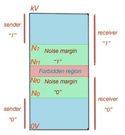
The noise margin is the difference between the absolute value of the output signal and the forbidden region of the receiver. The noise margin for level 0 is . The noise margin for level 1 is nm1 = N1 – Nf1. If Nm0 = nm1, then noise margins are symmetric. These conditions guarantee that the digital devices, sender and receiver will communicate properly. It is always good to design new devices to maximise these noise margins.