
FET transistors are working differently than BJT transistors. In FET width of conducting channel is varied by applying of external electric field. They operate similarly to the voltage-controlled resistors.
FET transistors can be divided into three groups:
- MOSFET, metal-oxide-semiconductor field-effect transistor;
- enhancement-mode MOSFET and depletion-mode MOSFET;
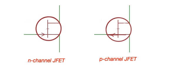
- junction field-effect transistor, JFET.
Each group can also be subdivided into n-channel and p-channel types.
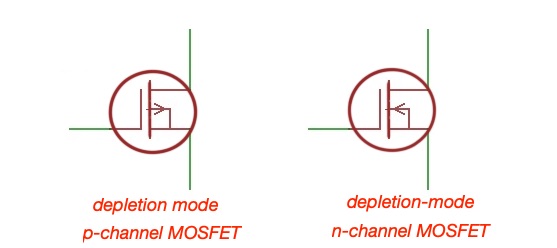
Figure below shows electrical signs of different types of Field-effect transistors.
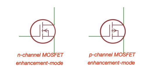
Enhancement MOSFET
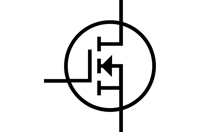
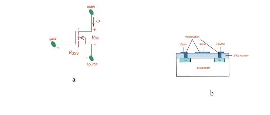
An N-channel enhancement mode MOSFET schematic is depicted in Figure 1. It is constructed of two materials – p- and n-type semiconductors. The MOSFET consists of three zones – gate, drain and source, and also the bulk or substrate is electrically connected to the gate.
The gate itself is a metal layer on the semiconductor substrate. The drain is connected to the voltage supply VDD, the source is connected to the ground, and the substrate is connected to the ground.
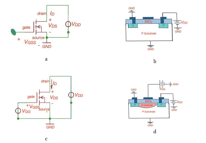
When the gate voltage is 0V, the path between the drain and source is reverse biased, no current flows through it, and is off. This is a cutoff regime – Figure 2. When the positive voltage is applied to the n-type enhanced MOSFET, there is a narrow layer of the negative charge that appears on substrate, where the negative charge goes between the drain and source. The voltage generated between the drain and source should exceed the threshold level voltage VT.
The greater voltage applied to the gate, the deeper conduction channel. It is narrower near the drain and wider near the source. The current direction ID is from the drain to the source – the drain current. Let’s imagine that the source-drain voltage VSDis fixed, but the source-gate voltage VSG is increasing – the conducting layer width will grow, it’s resistance will decrease until the moment that the source-gate voltage is equal to VT.
Until this moment the MOSFET operates like a voltage controlled resistor. When VSG becomes equal to VSD the width of the channel on the drain side becomes minimal. This regime is called pinch-off regime. As soon as the pinch-off regime occurs the current ceases to grow, and the MOSFET operates as a constant-current source, and the drain current is limited by the saturation value.
The operation of a MOSFET before the pinch-off is called ohmic, the operation of a MOSFET after pinch-off is called saturation. If the drain-source voltage VDS reaches the breakdown level VB, the drain current rapidly increases and the device is destroyed. This region is called a breakdown region.
A very important characteristic you can find in the MOSFET datasheet is a drain current versus drain-source voltages. This is called drain characteristic curves.
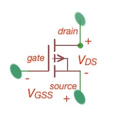
A P-type enhancement mode MOSFET schematic is depicted in Figure 3. Here, compared to a n-channel MOSFET, the direction on the drain current is opposite, the VGS and VDS have the opposite sign. The carriers are the holes and the channel is p-type. It explains why p-channel MOSFETS are slower than the n-type ones. So p-type MOSFETs are usually in use in complimentary devices – so called complimentary metal-oxide-semiconductor devises (CMOS devices).
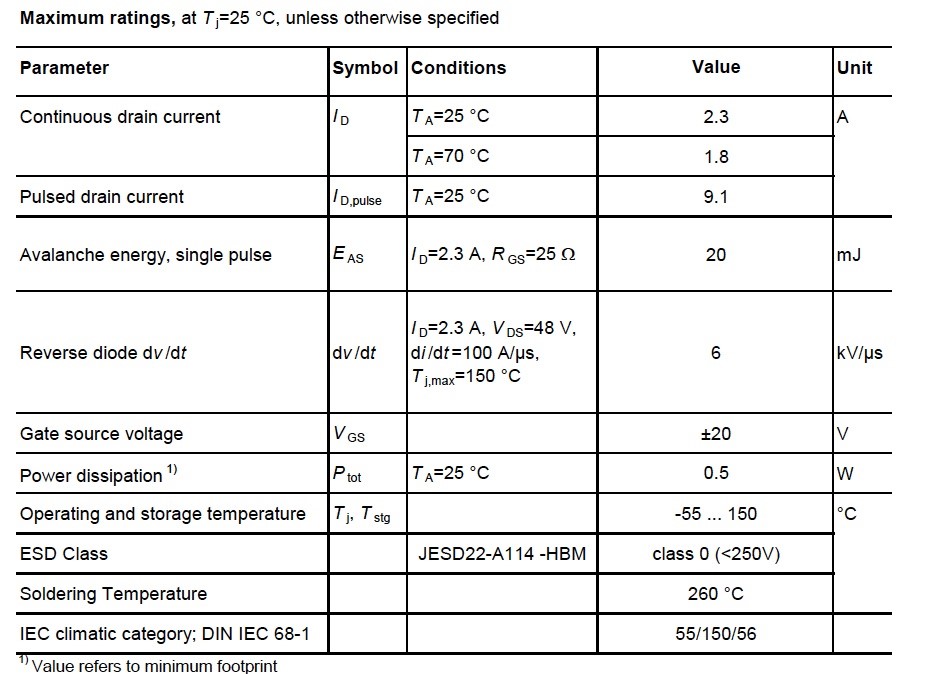
What’s in the datasheet? Let’s consider the enhancement type MOSFET SSM6K202FE from Toshiba. The first table we see show the maximum ratings. This data is most important when you design a circuit, they are not standardised and vary from manufacturer to manufacturer.
The maximum ratings is calculated data, it is not a result of an experiment or testing of the MOSFET, they are related to the circuit condition as a whole structure, it’s thermal characteristics and so on. Even if the operation parameters are in the range of the maximum ratings, using MOSFET with heavy loads (high temperature, current or voltage), may lead to massive MOSFET degradation.
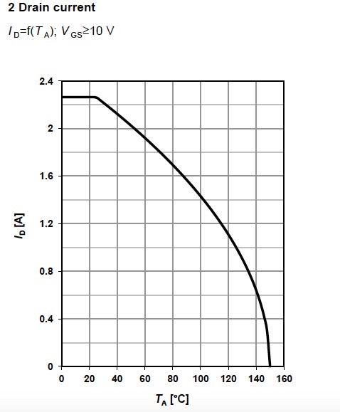
Maximum ratings can not be exceeded in order to support the device’s normal operation during it’s lifetime. Let’s consider in detail the maximum ratings. Drain current, is current that can pass through the MOSFET in the forward direction, ID, and pulsed drain current is current that can pass through the MOSFET in the forward direction IDpulse Some manufacturers also mention currents in reverse direction. The maximum continuous drain current depends on the power dissipation and is defined by the formula . The datasheet provides the graph for drain current ID(TC).
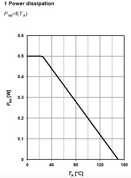
Above we referred to the Power dissipation of the device. The power dissipation graph is depicted in Figure 6 and power dissipation ratings are also mentioned in the maximum ratings table. There are two types – total junction-to-case and total-junction-to-ambient power dissipation. The junction-to case thermal resistance RthJC depends on the material and dimensions. The junction-to-ambient thermal resistance RthJA depends on the layout. The total power dissipation values can be obtain by the formula .
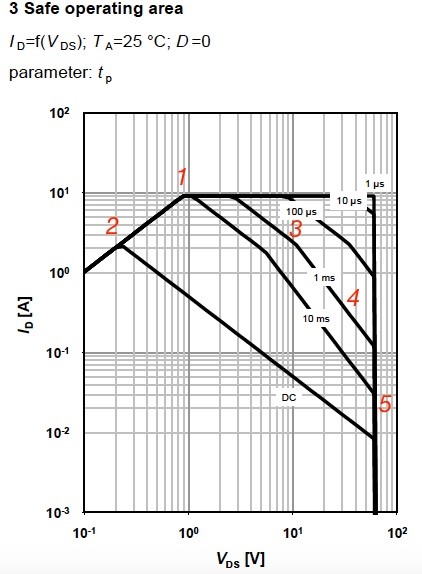
Safe operation area (SOA) graph, Figure 7, shows the drain current as a function of drain-source voltage with different pulses lengths. This is a very important graph that describes the regions of operation of the MOSFET (we considered above) and also it’s limits.
Line is a limit of the maximum ID,pulse. Area is limited by an on-state resistance at the maximum junction temperature. In Area , when case temperature TC is fixed, the device is limited by the constant power. Depending on the applied power pulse width, maximum power loss varies according to thermal impedance.
In Area , in linear mode operation, there is a risk of hot spots at low gate-source voltages due to thermal escape. This effect is very important for the latest technologies – for hot spots with high VDS and long pulses SOA described by the formula: . Region , shows the maximum breakdown voltage VBR(DSS), that is determined by technology.
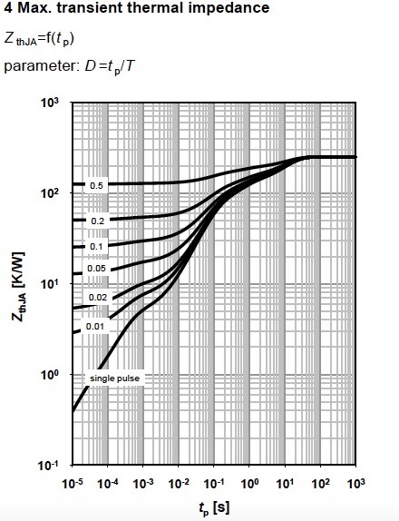
Maximum transient thermal impedance ZthJC. Thermal impedance consists of thermal resistance Rth and thermal capacitance Cth. The transient thermal impedance ZthJC takes into account the thermal resistance from the junction to the die of the case RthJC (this is the power loss in the device), and heat capacity CthJC.
The maximum transient thermal impedance as a function of the loading time tp (or the pulse width) is depicted in Figure 8. This graph shows different duty cycles . The MOSFET device consists of several layers, and heat is passing through all of them (each layer has characteristic resistance and capacitance).
Heat dissipation will depend on the thermal resistances, thermal capacitances and pulse width. The junction temperature can be obtained by the formula ,
where Tj,start is the TC at th thermal equilibrium.
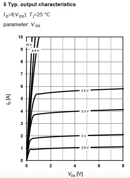
The next graph in the datasheet is output characteristics, (Figure 9) which describes drain current ID, as a function of the drain-source voltage VDS at certain conditions. This graph depicts ohmic regions, and this is where a MOSFET operates at its optimum. This graph is divided to two parts – ohmic and saturated regions.
The saturated region starts when VDS = VGS – VGS(th). Operation at the saturation region of the MOSFET is dangerous, because when the increases in this location, the VDS increases gradually, which leads to the rise of conduction losses, and the MOSFET may fail. The range of VGS mentioned in the datasheet determines the output characteristics graph.
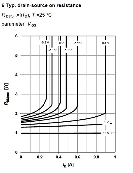
Drain-source on state resistance RDS(on) graphs are next in the datasheet. The drain source on state resistance RDS(on) as a function of drain current ID is calculated from the output characteristics curves with the formula . This curve changes massively depending on the applied VGS (Figure 10).
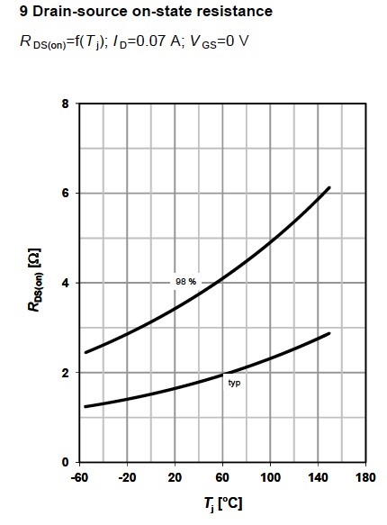
Drain-source on state resistance RDS(on) as a function of junction temperature . Figure 11 shows the typical and maximum values for resistance, and they are determined after production testing. The data set for RDS(on) can be calculated by the formula: , is a technology constant.
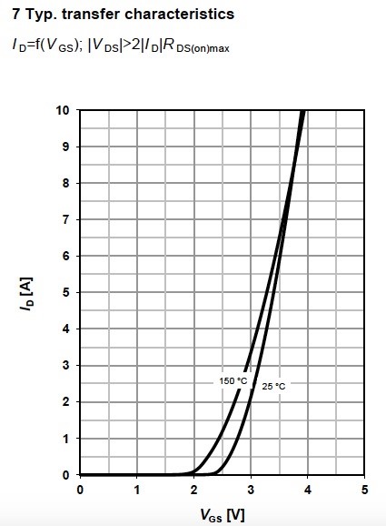
Typical transfer characteristics graph (Figure 12) shows the typical drain current as a function of source-gain voltage VGS at different junction temperatures. There can be more than two curves, and all of them are intersected at the point called temperature stable operating point.
When the VGS is below this point, the MOSFET is characterised by positive temperature coefficient. Then junction temperature Tj growth leads to drain current ID rise. The operation with constant VGS may fail the device because of thermal escape. When the VGS is bigger than the operating point value, then the thermal coefficient is negative, the rise of junction temperature Tj will decrease the drain current ID. The MOSFET operating in this interval should perform well as soon as Tj is within the datasheet limits.
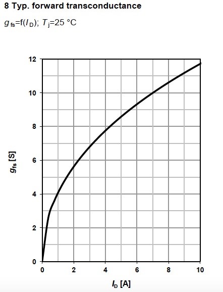
The datasheet shows Typical forward transconductance (Figure 13), gfs that is the measure of sensitivity of the drain current ID to the deviation of the gate-source voltage VGS. It can be obtained by the formula .
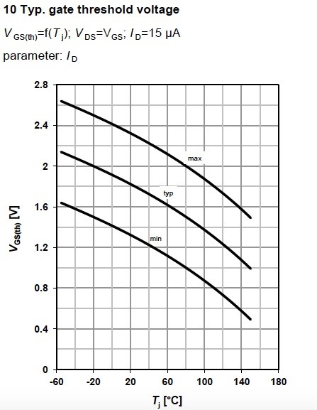
Gate threshold voltage VthGS (Figure 14), shows the required gate-source voltage VGS at a specific drain current ID. The threshold voltage is measured during production when VGS = VDS at specific drain current. You can find this data in the maximum ratings table.
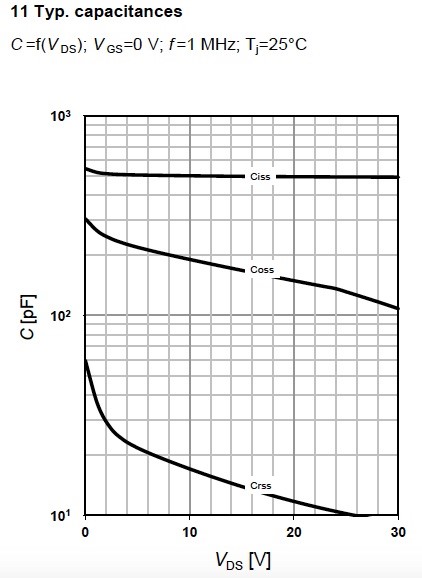
The dynamic characteristics table shows the Capacitances for the MOSFET – input, output and reverse transfer capacitances. They are described by the formulas: . Figure 15 shows input, output and reverse transfer capacitances and are shown as a function VDS.
Here we’ve considered the most important characteristics of the N-type depletion MOSFET. However, the order and the quantity of graphs and data may vary from vendor to vendor.
(BSR606N datasheet, Infineon, www.infineon.com; Infineon OptiMOS MOSFET datasheet explanation, www.infineon.com)


